JART – Jülich Aachen Resistive Switching Tools

Our laboratories provide simulation models for resistive switching devices to the scientific community. A focus on this dissemination activity are compact models to be used by circuit designers or device engineers. In the future, however, also kinetic Monte Carlo and continuum models will be provided. Please feel free to download the JART source codes. We request that you include a proper citation of either the web page or, preferentially, the corresponding papers whenever you are using it.
Recently we have also written a User Guide for the VCM model versions v1b, v1b var and v1b RTN. which can be downloaded here (User Guide PDF). We hope that this will aid new users of the compact models in getting acquainted with the models behavior as well as in learning more about the reasoning behind them.
Contact: jart@iwe.rwth-aachen.de
JART ECM v1
Short description:
The JART ECM v1 model describes the switching dynamics of Electrochemical Metallization Cells, which are also known as Conductive Bridge RAM (CBRAM) or atomic switches. The model includes the redox-reactions at the metal insulator interfaces, ion hopping transport, and the electrocrystallization of the filament nucleus (see Figure 1). The conduction mechanism is modeled here as an electron tunneling process. The model was originally developed to model the switching dynamics of a Ag/AgI/Pt device [1]. Later it was applied to GeSx based ECM cells [2] and a Ag/SiOx based system [3].
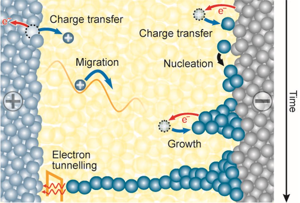
Figure 1: Ionic and Electronic process included in the JART ECM v1 model.
The Verilog-A code of this model can be downloaded here (Verilog-A file).
- [1] S. Menzel, S. Tappertzhofen, R. Waser and I. Valov, Switching Kinetics of Electrochemical Metallization Memory Cells, PCCP 15, 6945-6952 (2013).
- [2] J. van den Hurk, S. Menzel, R. Waser and I. Valov, Processes and Limitations during Filament Formation and Dissolution in GeSx-based ReRAM memory cells, J. Phys. Chem. C 119, 18678-18685 (2015).
- [3] M. Luebben, S. Menzel, S. G. Park, M. Yang, R.Waser and I. Valov, SET kinetics of electrochemical metallization cells - Influence of counter electrodes in SiO2/Ag based systems, Nanotechnology 28, 135205/1-6 (2017).
S. Menzel, C. Bengel
JART VCM v1
Short description:
The JART VCM v1 model was developed to simulate the switching characteristics of devices based on the valence change mechanism (also called OxRAM). In this model, the ionic defect concentration (oxygen vacancies) in the disc region close to the active electrode (AE) (see Figure 1) defines the resistance state. The concentration changes due to the non-isothermal drift of the ionic defects. In this model, Joule heating is considered, which significantly accelerates the switching process at high current levels.
The model was developed to study the two-step SET process of VCM cells [1] and the influence of an intrinsic series resistance on the switching characteristics [2].
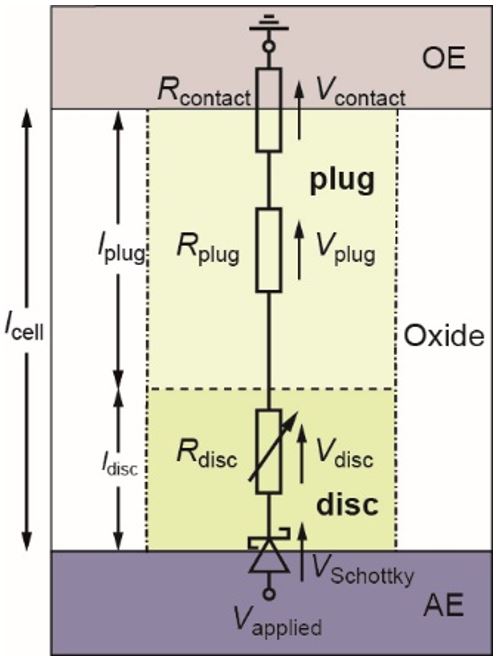
Figure 1: Equivalent circuit diagram of the JART VCM v1 model.
The Verilog-A code of this model can be downloaded here (Verilog-A file). In addition, we provide a stand-alone MATLAB App (here). To use the MATLAB app the downloaded file needs to be executed. During the first installation, the MATLAB runtime environment will be downloaded from the internet.
JART VCM v1 STO parameter set
The JART VCM v1 model can be used for different filamentary bipolar resistive switching material systems based on the Valence Change Mechanism. A different parameter set for this model is displayed in Table 1. It has recently been fitted again to the STO cells presented in [1].
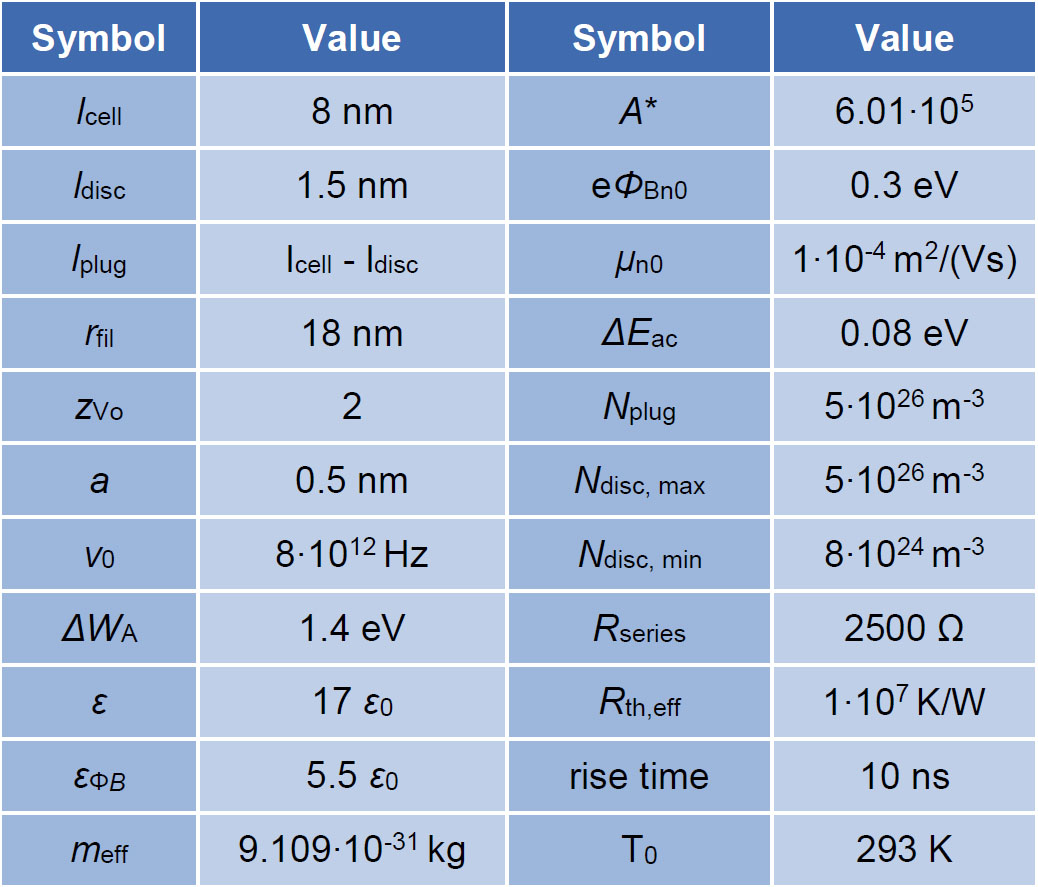
Table 1: Parameter set for STO.
The results from Figure 2 can be obtained by exchanging the fitting parameters with the ones in Table 1.
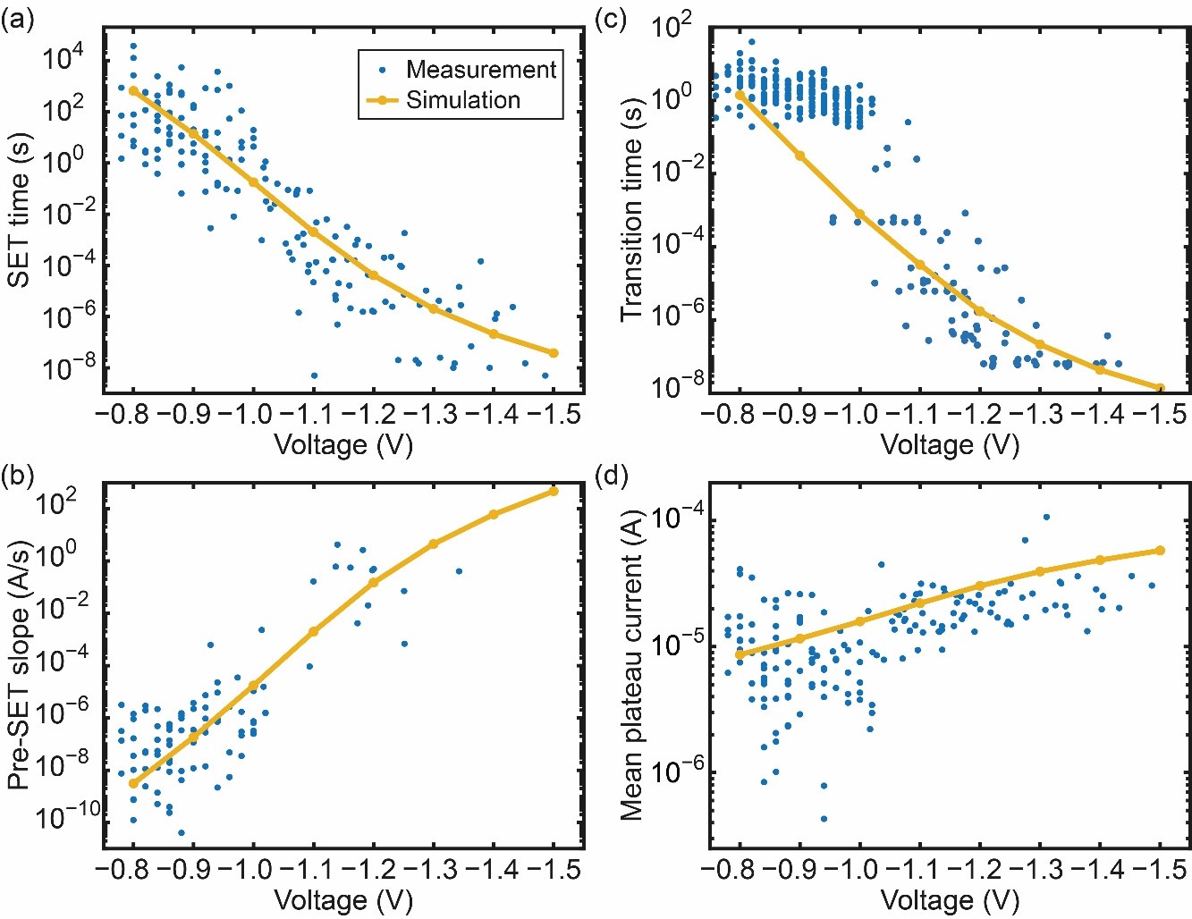
Figure 2: Highly voltage-dependent characteristic numbers of SET pulse switching, obtained with both experiments and simulations [3]. The simulation differs from the published result in [1] regarding the parameters, the definition of the criteria, and Eqs. (3.5), (3.7) to (3.10) and (3.12). (a) SET time to characterize the abrupt SET event. (b) Pre-SET slope of the linear degradation prior to the SET event. (c) Transition time to determine the speed of the abrupt SET event. (d) Mean plateau current used as additional information for fitting purposes.
- [1] K. Fleck, C. La Torre, N. Aslam, S. Hoffmann-Eifert, U. Böttger and S. Menzel, Uniting Gradual and Abrupt SET Processes in Resistive Switching Oxides, Phys. Rev. Applied 6, 064015 (2016).
- [2] A. Hardtdegen, C. La Torre, F. Cüppers, S. Menzel, R. Waser and S. Hoffmann-Eifert, Improved Switching Stability and the Effect of an Internal Series Resistor in HfO2/TiOx Bilayer ReRAM Cells, IEEE Trans. Electron Devices 65, 3229-3236 (2018).
- [3] C. La Torre, Physics-Based Compact Modeling of Valence-Change-Based Resistive Switching Devices, Dissertation RWTH Aachen, pp. 48 ff. 2019.
S. Menzel, C. Bengel
JART VCM v1b
Short description:
The JART VCM v1b model represents an improvement of the JART VCM v1 model. The ECD can be seen in Fig. 1. Some of the equations have been modified and the parameters have been fitted to describe the switching dynamics of HfOx based ReRAM devices. This contains the SET and RESET kinetics with a special focus on the initial states before the SET and RESET. This update leads to a better match of the SET and RESET processes as well as the I-V characteristic with the high resistive state (HRS) and the low resistive state (LRS), compared to the JART VCM v1 model [1].
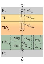
Figure 1: Equivalent Circuit diagram of the JART VCM v1b model.
Figure 2 shows some of the obtained results using this model. In Figure 2(a) the comparison of the experimental SET kinetics with the deterministic model is shown. The experimental SET delays are for initial LCS between ~2–10 μS. The initial LCS for the deterministic model were between 3-10 μS. Figure 2 (b) to (d) show the comparison of the experimental RESET behavior with the simulated RESET behavior. The model reproduces the connection between initial HCS and corresponding delay time (tRESET) very well for all considered cases. In addition, it shows a very good quantitative agreement concerning the shapes of the current transients.
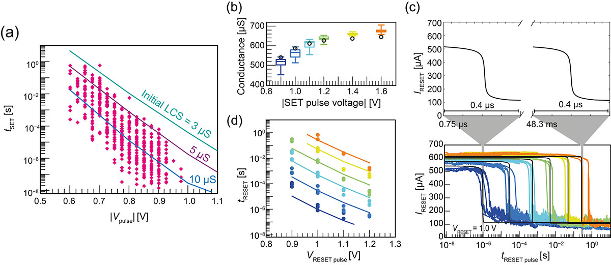
Figure 2: a) SET switching kinetics study revealing the variability of the experimental delay time for a given SET voltage. The solid colored lines displaying the deterministic simulations show that a large part of the delay can be attributed to the variation of the initial HRS. (b) shows the fit of the deterministic model to various HCS states. The black circles show the initial state that are used for the simulation in (c). In (c) the RESET current transients at a constant RESET voltage of 1 V are shown for those different initial HCS. The solid black lines represent the simulations that show that the simulated delay for a specific initial LRS very closely matches the experimental delay for a specific initial HCS. In (d) the RESET switching kinetics for various HCS are displayed. The difference in the delay as a function of the initial state can reach up to 6 orders of magnitude, which is reproduced by the model.
The Verilog-A code of this model can be downloaded here (Verilog-A file).
The User Guide for this model version can be downloaded here (User Guide PDF).
- [1] F. Cüppers, S. Menzel, C. Bengel, A. Hardtdegen, M. von Witzleben, U. Böttger, R. Waser and S. Hoffmann-Eifert, Exploiting the switching dynamics of HfO2-based ReRAM devices for reliable analog memristive behavior, APL Materials, 7, 091105, 2019.
S. Menzel, C. Bengel
JART VCM v1b var
Short description:
The JART VCM v1b var model represents an extension of the JART VCM v1b model which additionally considers device-to-device and cycle-to-cycle variability. The ECD can be seen in Fig. 1. The physical equations are the same as in the v1b model. Device-to-device variability is achieved through parameter variation of specific parameters during initialization of the devices and cycle-to-cycle variability is achieved through modification of the same parameters during the simulation run [1].
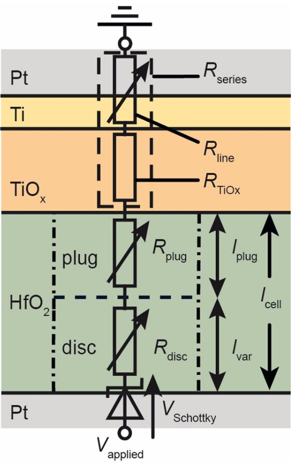
Figure 1: Equivalent Circuit diagram of the JART VCM v1b var model.
Characteristic figures used to describe VCM cells include the I-V characteristic, which can be used to determine the range for LRS and HRS as well as the ranges of SET and RESET voltages. Experimental I-V sweeps for a current compliance of 100 μA are shown in Fig. 2 (a) whereas Fig. 2 (b) shows the simulation result. Both sweeps were performed using the same sweep rate (1 V/s) and the same stop voltages for SET and RESET of ±1.3 V. The SET voltages are between −0.45 V and −0.75 V, while the RESET voltages are between 0.45 V and 0.65 V. Fig. 2 (c) shows the measured SET delays, i.e. the time required to switch the cell into the LRS for a voltage pulse of a specific height between −0.6 V and −1.1 V. Fig. 2 (d) shows the simulated SET kinetics. The variability model reproduces the non-linearity as well as the multiple orders of magnitude variation in the SET time. Fig. 2 (e) shows a more complex experiment, which could be reproduced using the proposed model, namely the RESET kinetics for different initial LRS. For this experiment, the devices were first SET using different SET voltages which resulted in different LRS states. Afterward, a RESET kinetic was measured from those different LRS. Fig. 2 (g) shows the measured endurance characteristic over 1000 SET-RESET cycles. The LRS turns out to be very stable at around 3 kΩ, while the HRS varies between 30 kΩ and 100 kΩ with only a few outliers above 100 kΩ. Fig. 4 (h) shows the simulated endurance behavior over 1000 cycles. The LRS again is rather stable with a slightly larger variability than the experiment around 3 kΩ, while the HRS varies between 20 kΩ and 100 kΩ.
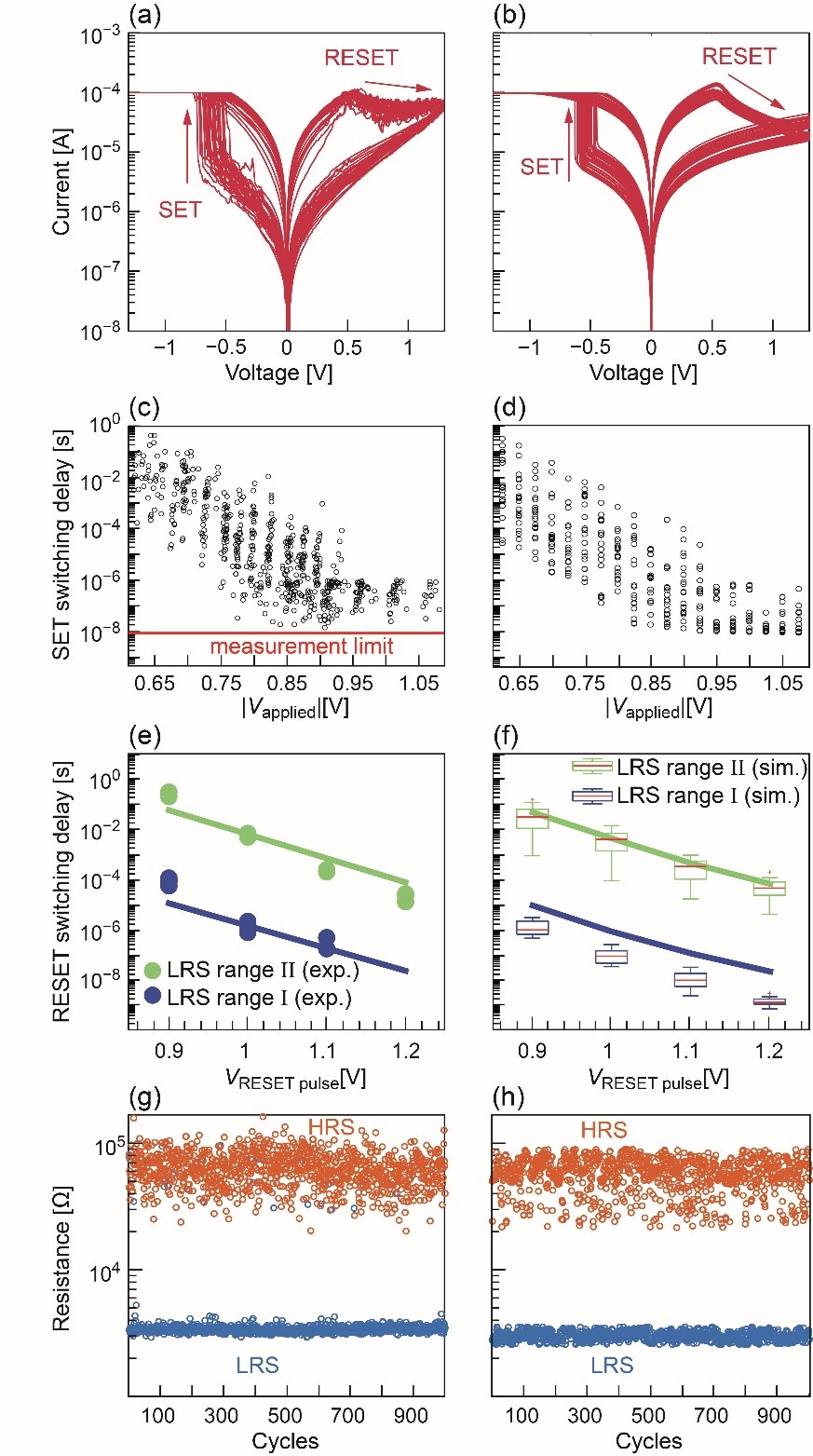
Figure 2: Measured device characteristics alongside results obtained using the extended compact model. The first row shows measured (a) and simulated (b) voltage sourced I-V sweeps. The second row shows the measured (c) and simulated (d) SET kinetics and the third row shows the measured (e) and simulated (f) RESET kinetics. The blue circles represent the experimental RESET kinetics starting from LRS between 1.85 kΩ and 2.22 kΩ (LRS range I (experimental)) while the green points represent the RESET kinetics starting from LRS between 1.52 kΩ and 1.67 kΩ (LRS range II (exp.)). The solid lines represent the RESET kinetics of the deterministic model using the parameters from Table I and the initial LRS as detailed in [1]. The blue box plots show the RESET kinetics for the variability model for an LRS range between 1.92 kΩ and 2.04 kΩ (LRS range I (simulated)) while the green box plots show the RESET kinetics of the variability model for an LRS range between 1.58 kΩ and 1.67 kΩ (LRS range II (sim.)). The fourth row ((g) and (h)) shows the measured and simulated endurance behavior over 1000 cycles. Generally, a good qualitative agreement between measurement and simulation is observed not only for device properties like LRS, HRS, SET and RESET voltages and switching kinetics but also for the statistical behavior of these properties.
The Verilog-A code of this model can be downloaded here (Verilog-A file). The User Guide can be downloaded here (User Guide PDF).
- [1] C. Bengel, A. Siemon, F. Cüppers, S. Hoffmann-Eifert, A. Hardtdegen, M. von Witzleben, L. Hellmich, R. Waser and S. Menzel, Variability-Aware Modeling of Filamentary Oxide-Based Bipolar Resistive Switching Cells Using SPICE Level Compact Models, IEEE Trancsactions on Circuits and Systems-I, VOL. 67, NO. 12, 2020.
S. Menzel, C. Bengel
JART VCM v1b Readvar
Short description:
The JART VCM v1b Readvar model represents a further extension of the JART VCM v1b var model which additionally considers read noise. The ECD can be seen in Fig. 1 [1]. The read noise is implemented by adding a random jump of single oxygen vacancies to and from the disc region directly resulting in a jump of the measured resistance.
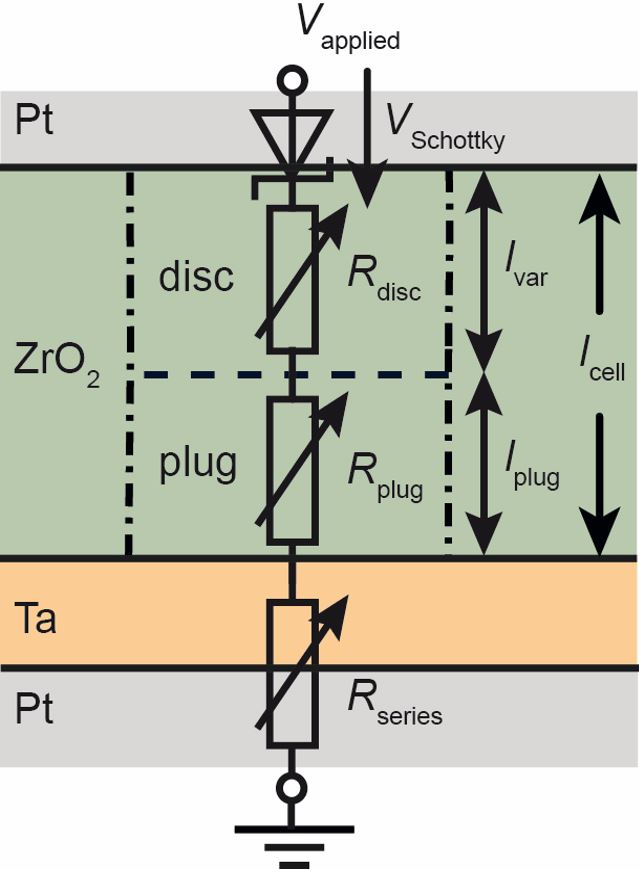
Figure 1: Equivalent Circuit diagram of the JART VCM v1b Readvar model.
Figure 2 shows a set of current traces of different devices measured at a read voltage of 0.35 V. As can be observed diferent devices can exhibit different jump frequencies. The current jump height is thereby a function of the average resistance with higher resistances resulting in higher jumps on average.
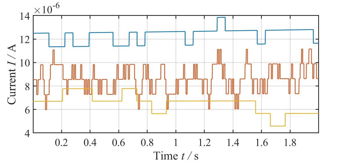
Figure 2: Simulated current tracesmeasured at 0.35 V. The signals all show the characteristic current jumps between distinct levels around a constant median current.
The Verilog-A code of this model can be downloaded here (Verilog-A file). The User Guide can be downloaded here (User Guide PDF).
- [1] S. Wiefels, C. Bengel, N. Kopperberg, K. Zhang, R. Waser and S. Menzel, HRS Instability in Oxide-Based Bipolar Resistive Switching Cells, IEEE Transactions on Electron Devices, VOL. 67, NO. 10, 2020.
S. Menzel, C. Bengel
JART VCM v1 generic
Short description:
The JART VCM v1 generic model is a special variant of the more general JART VCM v1 model. It provides in total 16 data sets to study the influence of the nonlinearity SL of the switching kinetics and the resistance ratio r on different circuit designs [1]. Four different slopes and four different resistance ratios can be chosen. To simplify the comparison, the different slopes intersect at about 1 µs (cf. Figure 1). Thus, the same voltage amplitude and pulse length can be used in a circuit when changing the slope. When increasing the resistance ratio, however, the required switching voltages increases, which is consistent with experimental observations (Fig. 1c, d). To allow for this comparison, the JART VCM v1 model is slightly modified: the electronic transport is assumed to be temperature-independent.
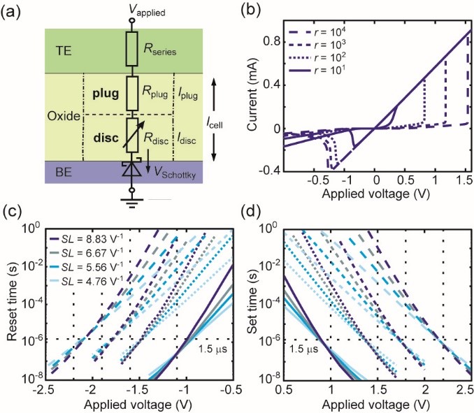
Figure 1: (a) Equivalent circuit diagram of the simulation model showing the top electrode (TE), the bottom electrode (BE) and the active oxide layer. (b) Simulated I-V characteristics all resistance ratios r and the nonlinearity SL = 8.83 V-1. (c) Reset and (d) set times vs. applied voltage for all combinations of r and SL. [1].
The Verilog-A code of this model can be downloaded here (Verilog-A file). The following small errors should be noted:
Typos in Table 2 of the paper:
Unit of A* should be A/(m2*K2)
Nplug should be 25*1026 m-3
Typo in Figure 1 (b) on the x-axis: -1 V and -0.5 V are switched.
- [1] A. Siemon, D. J: Wouters, S. Hamdioui and S. Menzel, “Memristive Device Modeling and Circuit Design Exploration for Computation-in-Memory”, 2019 IEEE International Symposium on Circuits and Systems (ISCAS), Sapporo, Japan, 26-29 May, 2019.
S. Menzel, C. Bengel
JART VCM v2
Short description:
The JARV VCM v2 model is an extension of the JART VCM v1 model. It includes two different switching locations I and II (see Figure 1). Thus, the model uses two state variables. In addition, diffusion between region I and II is included in this model, enabling the simulation of retention. The model was developed to simulate complementary switching and bipolar switching in a single device [1].
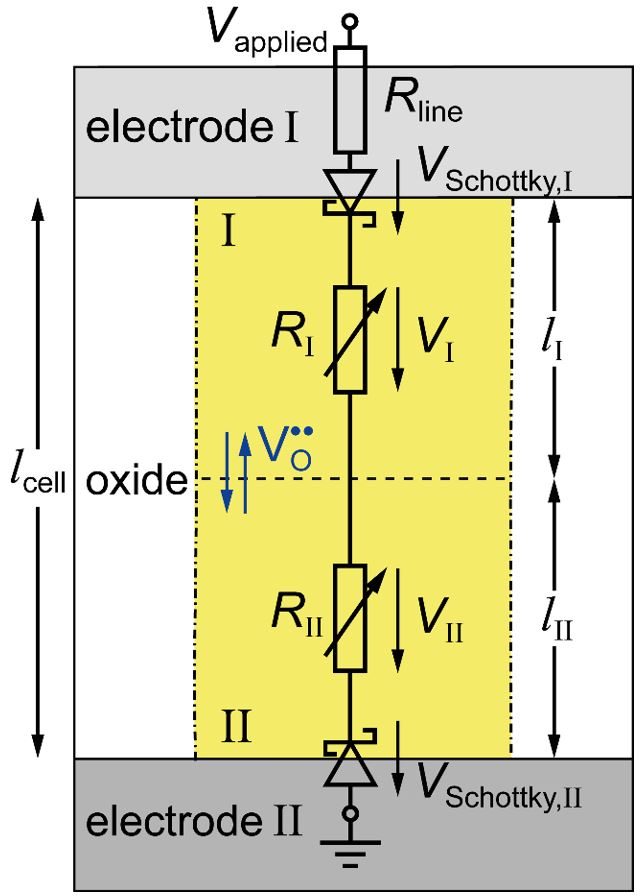
Figure 1: Equivalent circuit diagram of the JART VCM v2 model.
The Verilog-A code of this model can be downloaded here (Verilog-A file). In addition, we provide a stand-alone MATLAB App (here). To use the MATLAB app the downloaded file needs to be executed. During the first installation, the MATLAB runtime environment will be downloaded from the internet.
- [1] C. La Torre, A. F. Zurhelle, T. Breuer, R. Waser and S. Menzel, Compact Modeling of Complementary Switching in Oxide-Based ReRAM Devices, IEEE Trans. Electron Devices 66, 1268-1275 (2019).
S. Menzel, C. Bengel
JART OxRelax
Dynamics of the spatial separation of electrons and mobile oxygen vacancies in oxide heterostructures
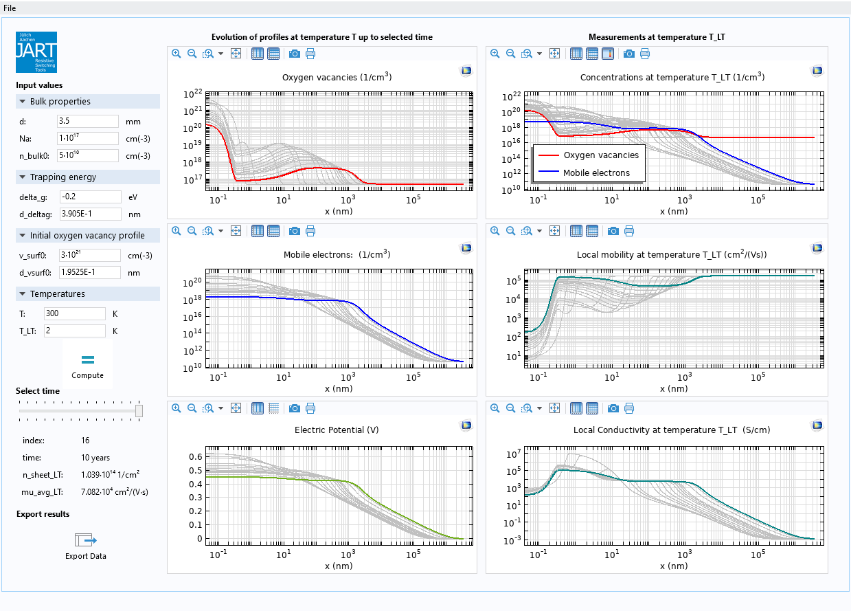
In the search for an oxide-based 2D electron system with a large concentration of highly mobile electrons, a promising strategy is to introduce electrons through donor doping while spatially separating electrons and donors to prevent scattering. In SrTiO3, this can be achieved by tailoring the oxygen vacancy profile through reduction, e.g., by creating an interface with an oxygen scavenging layer. Through reduction, oxygen atoms are removed close to the interface, leaving behind oxygen vacancies in the SrTiO3 lattice and mobile electrons in the SrTiO3 conduction band. The commonly assumed picture is that the oxygen vacancies then remain confined close to the interface while the electrons leak a few nanometers into the bulk, resulting in an electron-defect separation and a highly mobile, oxide-based 2D electron system.
Here, we present a transient finite element simulation tool that describes how the concentration profiles of oxygen vacancies and electrons develop over a timescale from minutes to 10 years at temperature T. This tool considers three driving forces acting on the oxygen vacancy distribution: diffusion due to the concentration gradient, drift due to the intrinsic electric field, and an oxygen vacancy trapping energy that holds oxygen vacancies at the interface. Furthermore, this tool provides data that can be compared to conductivity measurements at a second temperature TLT.
This COMSOL App is available without (small – 15 MB) and with (large – 744 MB) COMSOL runtime. In the first case, the download is significantly smaller and the COMSOL runtime will be automatically installed if necessary.
- [1] A. F. Zurhelle, D. V. Christensen, S. Menzel, and F. Gunkel, Phys. Rev. Materials 4, 104604. DOI: 10.1103/PhysRevMaterials.4.104604
A. F. Zurhelle