Probing the nanoworld - scanning probe techniques and more
Progress in nanoscience and nanotechnology is closely related to the evolution of novel techniques in experimental analysis. Tip-based scanning probe systems represent the work horses of our equipment at the EMRL for probing nanoscale structures and objects with atomic resolution, comprising dedicated environments such as local conductivity microscopy (LC-AFM), tunneling microscopy (STM) and conductance spectroscopy (STS) of low-dimensional structure on oxide surfaces and of molecular systems, piezoresponse force microscopy (PFM) of polar oxide nanostructures and ferroelectric domain configurations. This is complemented by looking into our electronic materials and fabricated nanostructures using our close ties with the Ernst Ruska-Centre for ultra-high resolution transmission electron microscopy and spectroscopy as well as with institutes of JARA-FIT which operate modern synchrotron beam lines for a multitude of analytical techniques for the investigation of structural and electronic properties of electronic materials.
Investigation of the Filament Growth in TiO2 Memristive Junctions with Conductive Atomic Force Microscopy
Resistive switching in transition metal oxides has been studied for quite some time now and occurs within a wide variety of materials. The actual microscopic processes, however, are not yet completely understood. Although there are several conceivable mechanisms, in recent time there have been more and more indications that the oxidation and reduction of conducting filaments close to the anode interface seem to be responsible for the resistance change [1-3]. A common feature of most switching materials is the necessity of an initial electroforming step before stable resistive switching can be realized. In the case of TiO2 devices it could be shown that this forming step is related to the irreversible formation of a reduced, conducting path through the junction [4]. Understanding the exact influence of this forming step as well as the influence of subsequent switching steps on the junction and, moreover, being able to distinguish between both of them, is clearly an important prerequisite for understanding the overall switching process.
We present here conductive atomic force microscopy (C-AFM) studies of TiO2 memristive junctions enabled by a delamination process. By removing the top electrode while still keeping the chemical integrity of the processed devices, we were able to investigate the TiO2/electrode interface and detect the effects of the electroforming on the local conductivity of the sample. A comparison of samples that were only electroformed to samples that were additionally switched allowed us to extract the influence of subsequent switching steps on the morphology and conductivity of the sample. Our samples consist of a Ti(5 nm)/Pt(15 nm)/TiO2(30 nm)/Pt(30 nm) stack sitting on a Si/SiO2 wafer. In order to directly investigate the influence of forming as well as switching on the sample we removed the top electrode and took a direct look at the active TiO2 surface with C-AFM using a conductive diamond coated tip. Images showing the topography and local current distribution of a sample are denoted by a red “T” and “C”, respectively.
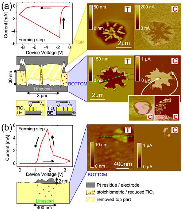
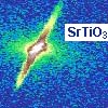
Figure 1: Influence of electroforming on the morphology and local conductivity of a sample. The I–V and C-AFM data of a sample formed by a negative (positive) voltage sweep are shown in part (a) (part (b)). The dashed green line marks the position of the linescan shown on the left hand side.
In order to proceed from its initially high resistive virgin state to a resistive switching state, a sample needs to be electroformed. This can be achieved by applying either a negative voltage sweep – resulting in the ON state – or a positive voltage sweep, resulting in the OFF state. Figure 1a contains the I–V data of a negatively formed junction. Upon delamination the structure falls apart into two pieces: a bottom part and a top part. The C-AFM images in Figure 1a show the topography and conductivity of both parts, while the green linescan as well as its coloured depiction below the I–V curve outline this separation. The C-AFM sample setup is sketched for the bottom as well as for the flipped over top part in the two small pictograms beneath. The bottom part exhibits a several micron sized hole situated somewhere across the junction area with an approximately 200 nm wide pillar in the middle and some elevated regions at the boundaries. The depth of the hole is equal to the TiO2 film thickness. The overall bottom part therefore consists of the bottom electrode with the complete oxide layer sitting on top - except for the hole; within the hole all TiO2 has been pulled out during delamination making the ground equivalent to the Pt bottom electrode. The top part is the exact counterpart of the bottom part. It consists of the small amount of TiO2 that was plucked out of the sample, sitting on top of the top electrode. Taking a closer look at the conductivity of both parts, the Pt top and bottom electrodes can be seen as very well conducting regions. The plucked TiO2 of the top part as well as the main part of the TiO2 in the bottom part image is non-conducting. The conductivity and therefore also stoichiometry of those areas was obviously not affected by the forming step. The only current carrying regions of the whole device are located at the central pillar and the boundary regions of the hole structure. Both possess an increased conductivity compared to the surrounding stoichiometric TiO2 film and are shown in the insets of Figure 1a. From their conductivity we infer that they consist of reduced TiO2. The height of the central pillar as well as the boundary regions is slightly larger than the film thickness, making them protrude above the average TiO2 surface. Photo Emission Electron Microscopy (PEEM) reveals that the boundary regions were crystallized during the electroforming step and that the central pillar is covered with a residual Pt layer - accounting for the additional height and preventing immediate reoxidation [5]. The whole very characteristic structure can be explained by the formation of an original conducting TiO2-x channel (central pillar) by Joule heating and oxygen vacancy migration together with the evolution of an oxygen bubble at the lower interface around this channel. This bubble delaminated the oxide film from the bottom electrode and eventually also broke the contact between the central channel and the top electrode. Further current flow occurred only along the boundaries of the bubble, heating and crystallizing them and therefore causing an increased adhesion between film and Pt electrode in these areas. The confinement of the current to the boundaries of the hole and the rupture of the central channel is also supported by local pressure modulated AFM measurements prior to removing the electrode [4]. Positive electroforming (Figure 1b) also results in a localized conducting region but the overall changes to the sample structure are much less dramatic. In this case a small conducting spot appears at the edge of the junction together with a roughly 400 nm wide and 2–3 nm high elevation in the topography. The region of the conducting spot also shows a heat-induced crystallization (as determined by PEEM) and likely reduction of the film with an increased adhesion to the top electrode and a small residual Pt layer.
Figure 2: Influence of resistive switching on the morphology and local conductivity of the sample. I–V and C-AFM data are shown for a sample negatively formed and switched once (a), a sample positively formed and switched once (b), and a sample positively formed and switched several times (c). In addition to the forming spot further conducting areas emerge due to the switching steps. They are marked by dashed rectangles.
While electroforming causes very characteristic changes to the film structure, stoichiometry and conductivity, subsequent resistive switching yields additional effects. Figure 2a shows the I–V characteristic and C-AFM data of a junction that has been formed by a negative voltage sweep – reaching the ON state – and then switched back into the OFF state by a positive sweep. While the electroforming step results in a hole structure similar to the one shown in Figure 1a, a secondary structure right next to where the hole is appears. It is marked by a dashed square in the topography image and its conductivity is shown in the (magnified) current image. It is conducting and exhibits the same slightly rough morphology as the reduced and Pt covered regions described above. By comparison with only formed samples we can determine that it originates from the switching sweep that followed the forming. A similar effect occurs for a positively formed sample (Figure 2b): while the initial forming results in a small conducting structure the subsequent switching causes additional conducting spots to appear. PEEM measurements confirm that in both cases the additional switching induced conducting regions are crystallized by Joule heating and their rough morphology probably results from residual Pt. The reason for the appearance of an additional current carrying region lies probably in yet another gas induced detachment of the electrodes from the respective channel during the first switching step. This idea of an ongoing breaking of existing current channels and creation of other ones during subsequent switching steps is furthermore supported by our data obtained from samples switched not only once but several times – as shown in Figure 2c. While a junction switched only once has a comparably small conducting structure (see Figure 2b), samples which were switched several times exhibit an elongated feature extending along the edge of either top or bottom electrode. Since the length of the conducting structure increases, when switching a junction several times, one should also expect an accompanying increase in current. However, no such increase has been observed. The value of the overall electrical resistance in either ON or OFF state is very stable and the resistive switching can be repeated many times without any remarkable drift of the states. Therefore we conclude that not the whole structure visible with C-AFM is actually carrying the current in the non-delaminated device. Rather a breaking of existing conducting channels (off of the top electrode, similar to the gas bubble induced breaking of the central pillar during negative forming) and a subsequent creation of a neighbouring channel occurs. This would also fit with the fact, that before delamination the electrode above the observed structure shows strong deformation not only at the forming spot but also in an extended region next to it hinting at gas evolution.
This research was funded in part by the US Government's Nano-Enabled Technology Initiative.
- [1] B. J. Choi et al., J. Appl. Phys. 98, 33715 (2005).
- [2] Kyung Min Kim et al., Appl. Phys. Lett. 91, 012907 (2007).
- [3] D. S. Jeong et al., Phys. Rev. B 79, 195317 (2009).
- [4] J. J. Yang, F. Miao, M. D. Pickett, D. A. A. Ohlberg, D. R. Stewart, C. N. Lau, and R. S. Williams, Nanotechnology 20, 215201 (2009).
- [5] J. P. Strachan, J. J. Yang, R. Münstermann, A. Scholl, G. Medeiros-Ribeiro, D. R. Stewart, and R. S. Williams, Nanotechnology 20, 485701 (2009).
Ruth Münstermann1, J. Joshua Yang1, John Paul Strachan1, Gilberto Medeiros-Ribeiro1, Regina Dittmann, and Rainer Waser
1 Hewlett-Packard Labs, 1501 Page Mill Road, Palo Alto, CA 94303, USA
Probing the Oxygen Vacancy Distribution in Resistive Switching Fe-SrTiO3 MIM-Structures by Micro-XANES
Resistive switching metal-insulator-metal (MIM)-structures were fabricated from epitaxial Fe-doped SrTiO3 thin films to study the distribution of oxygen vacancies in a switched memristor cell using a micro-focused x-ray beam. In addition to the main filament, we found that the concentration of oxygen vacancies increases homogeneously over the whole electrode area during the electroforming procedure. The XANES observed at the location of the filament exhibits distinct differences to the surrounding area, which are interpreted with full-multiple-scattering XANES calculations to derive from oxygen vacancy clustering in the first coordination shell around Fe.
Binary and ternary metal oxides as emergent materials for non-volatile memory applications are receiving an increasing amount of scientific attention due to the promising scalability, retention and switching characteristics of this material class [1]. The key role of oxygen non-stoichiometry and oxygen-deficient oxide-phases as the underlying mechanism of the resistance change has been recognized for many different oxide systems (e.g. TiO2, Ta2O5, SrTiO3). It is becoming widely accepted that the resistance switching process in SrTiO3 is related to the movement and creation of oxygen vacancies and the associated electron doping. However, direct experimental reports of the redox-reaction induced by an electric field are rare [2].
In this contribution, the distribution of oxygen vacancies in a switched memristor cell fabricated from epitaxial Fe-doped SrTiO3 will be investigated by spatially resolved x-ray absorption near-edge structure (XANES). SrTi0.95Fe0.05O3 was grown epitaxially by pulsed laser deposition (PLD) on a conducting Nb:SrTiO3 substrate. Pt top electrodes were sputter-deposited and structured via optical lithography. XANES measurements at the Fe K-edge with a 7 μm beam spot on the sample were performed at the beamline ID03 (ESRF, France). Figure 1 compares the Fe K-edge XANES of the virgin thin film to that recorded in the anodic and cathodic regions of an electrocolored single crystal [3]. The cathode was found to contain only Fe3+ ions and Fe3+-VO complexes in the ratio ~ 70/30, and notably no Fe4+ [3]. The almost perfect coincidence of the thin film XANES with that of the reduced cathode implies that the virgin thin film is already oxygen deficient after growth, and that the Fe3+/Fe4+ redox pair does not serve as an indicator for local resistance changes. The shoulder at 7122 eV excitation energy that marks Fe3+-VO complexes is indicated by “S” in Figure 1.
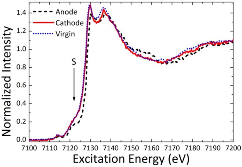
Figure 1: Fe K-edge XANES recorded on the virgin thin film (dots), the cathode region (solid) and the anode region (dash) of an electrocolored Fe-doped SrTiO3 single crystal. The intensity of the shoulder at 7122 eV excitation energy (marked S by the arrow) is a fingerprint of the presence of an oxygen vacancy in the first coordination shell of Fe3. The chemical state of the virgin film - according to the XANES - is similar to that of the cathode, and the Fe centers in the film are primarily cubic Fe3+ centers, with a significant percentage of axial Fe3+-VO centers.
After an electroforming step with a +7 V DC voltage applied to the top electrode, the formed memristor can be switched between different resistance states with a bipolar voltage sweep. The current-voltage hysteresis is shown in Figure 2(a), the “Set”-state is reached with a negative voltage sweep polarity. A low voltage readout (Figure 2(b)) reveals the “Set”-state to show ohmic behavior, while the “Reset”-state shows distinctly non-linear behavior.
A Fe-K edge fluorescence map recorded at 7122 eV excitation energy to maximize the sensitivity to Fe3+-VO reveals one location on the electrode pad with increased intensity, corresponding to the main filament. Moreover, the Fe3+-VO concentration as measured by the intensity of the shoulder S is increased under the whole electrode area as compared to the virgin film.
The important consequence is that before breakdown is achieved during the electroforming, a homogeneous front of vacancy enrichment propagates into the material. Furthermore, the Fe K-edge XANES at the filament location is interpreted via full multiple-scattering calculations and indicates oxygen vacancy clustering in the first shell of Fe [4]. The oxygen vacancy distribution in the formed device is sketched in Figure 3.
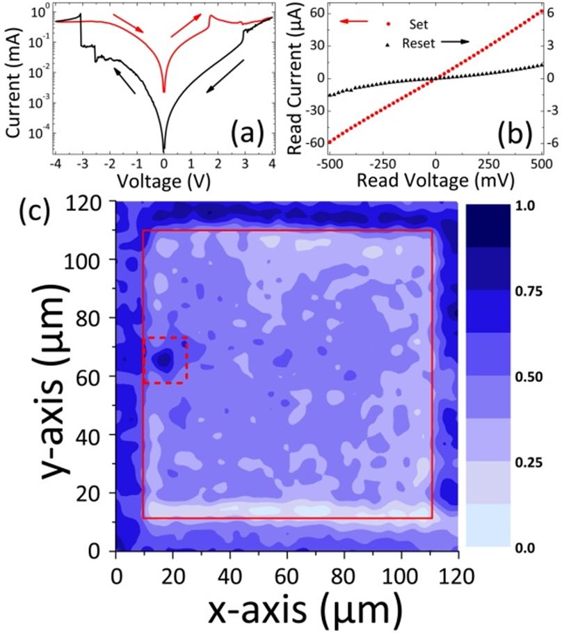
Figure 2 (a): I(V)-characteristics of the investigated memristor after electroforming. (b): Low voltage, non-destructive read-out sweeps in the low resistance “Set”-state (dots) and the high resistance “Reset”-state (triangles). (c): Fe K? fluorescence map of the switched memristor, recorded at 7122 eV excitation energy (shoulder S). The intensity variations under the electrode correspond to the oxygen vacancy content, the maximum in the dashed box indicates the presence of the conducting filament. The absolute intensity outside the electrode area (solid lines) is higher since the fluorescence radiation is not attenuated, but cannot be directly compared to the intensity under the electrode.
In summary, we have shown PLD-grown SrTi0.95 Fe0.05O3 thin films to contain Fe3+ and a high degree of Fe3+-VO complexes in the as-deposited state. We demonstrate through micro-focused XANES on a resistively switched MIM-structure that electroforming increases the Fe3+-VO complex concentration homogeneously over the whole electrode area until local breakdown is achieved. Full multiple-scattering XANES calculations suggest that the observed XANES in the region of the conducting filament can be interpreted by the association of two oxygen vacancies to the probed Fe in the filament region.
This work was financially supported by the EC FP7 MATERA project FMRSM and the NRW-EU Ziel 2-Programm.
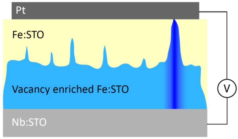
Figure 3: Schematic model of the oxygen vacancy distribution in the switched memristor.
- [1] R. Waser, R. Dittmann, G. Staikov, and K. Szot, Adv. Mater. 21, 2632 (2009).
- [2] M. Janousch, G. I. Meijer, U. Staub, B. Delley, S. F. Karg, and B. P. Andreasson, Adv. Materials 19, 2232 (2007).
- [3] C. Lenser, A. Kalinko, A. Kuzmin, D. Berzins, J. Purans, K. Szot, R. Waser, and R. Dittmann, Phys. Chem. Chem. Phys. 13, 20779 (2011).
- [4] C. Lenser, Ch. Lenser, A. Kuzmin, J. Purans, A. Kalinko, R. Waser and R. Dittmann, J. Appl. Phys. in press
C. Lenser, A. Kuzmin1, J. Purans1, A. Kalinko1, R. Waser and R. Dittmann
1 Institute of Solid State Physics, University of Riga, Latvia
Polarization and Lattice Strains in Epitaxial BaTiO3 Films Grown by High-Pressure Sputtering
High-quality BaTiO3 films with thicknesses ranging from 2.9 to 175 nm were grown epitaxially on SrRuO3-covered (001)-oriented SrTiO3 substrates by high-pressure sputtering. The in-plane and out-of-plane lattice parameters were determined as a function of film thickness by x-ray reciprocal space mapping around the asymmetric (̅103) Bragg reflection. BaTiO3 films were found to be fully strained by the SrTiO3 substrate up to a thickness of about 30 nm. Polarization-voltage hysteresis loops were recorded at the frequencies 1–30 kHz. The observed thickness effect on the lattice parameters and polarization in BaTiO3 films was analyzed in the light of strain and depolarizing-field effects using the nonlinear thermodynamic theory. The theoretical predictions are in reasonable agreement with the measured thickness dependences, although the maximum experimental values of the spontaneous polarization and the out-of-plane lattice parameter exceed the theoretical estimates (43 μC/cm2 vs. 35 μC/cm2 and 4.166 Å vs. 4.143 Å). Possible origins of the revealed discrepancy between theory and experiment are discussed.
The current trend towards the downscaling of microelectronic devices makes especially important the investigations of size effects on the physical properties of ferroelectric films. Barium titanate (BTO) is a classical ferroelectric material which was extensively investigated in bulk form in the past. It represents a good choice for experimental studies of the size effects in ferroelectric thin films because detailed comparison between observations and theoretical predictions is possible in this case. In particular, the nonlinear thermodynamic theory of epitaxial ferroelectric films can provide quantitative description of BTO films since the thermodynamic parameters of BTO crystals were recently determined with a good degree of precision [1]. This theory describes the influence of substrate-induced lattice strains on the polarization state of an epitaxial film and shows that these strains may induce the formation of new ferroelectric phases in BTO films and increase the spontaneous polarization largely. Moreover, several first-principles calculations were performed for ultrathin BTO films. The existence of a minimum film thickness for the stability of a single-domain ferroelectric state was predicted, below which it transforms into the paraelectric one owing to the depolarizing-field effect. Kim et al. showed that the film polarization strongly decreases in ultrathin films, but even the 5-nm-thick BTO film displays a well-defined polarization hysteresis loop [2].
For the better understanding of the nature of size effects in ferroelectric films, it is important to measure both the polarization and lattice parameters in a wide range of film thicknesses and to analyze their variations theoretically.
We report here such measurements for BTO films grown by high-pressure sputtering on SrRuO3-covered (001) oriented SrTiO3 substrates, with thickness ranging from 2.9 up to 175 nm. The surface of BTO films has a good degree of flatness, with an rms roughness of about 1.9 Å. In order to determine the lattice parameters of BTO films and to evaluate the substrate-induced strains, we performed the x-ray reciprocal space mapping (X-RSM) of our heterostructures around the asymmetric (103) Bragg reflection and the results for several different thicknesses are showed in Figure 1. The lattice parameters are shown in Figure 2a. It can be seen that the films are fully strained by the STO substrate up to a thickness of 30 nm. For the investigation of the ferroelectric properties of BTO films, plate-capacitor structures were fabricated and polarization-voltage hysteresis loops of BTO capacitors were recorded at frequencies 1–30 KHz using an aixACCT TF Analyzer 2000. When the film thickness t is in the range of 25 to 100 nm, the P-V loop has practically ideal rectangular shape, which reflects high quality of fabricated BTO films and the absence of nonferroelectric (“dead”) layers at the film/electrode interfaces. At the film thicknesses below 20 nm, the shape of P-V loops deteriorates progressively. The leakage current increases further in the thinnest fabricated film (t = 2.9 nm), but the capacitor is still not short-circuited. Although the hysteretic behavior disappears at t = 2.9 nm, the current-voltage dependence remains nonlinear.
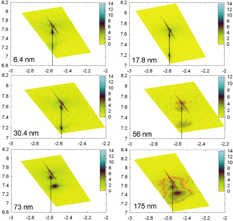
Figure 1: X-ray reciprocal space mapping (X-RSM) around the asymmetric (103) Bragg reflection for BaTiO3 films of several different thicknesses.
To describe quantitatively the influence of substrate-induced lattice strains on the orientation and magnitude of the spontaneous polarization, we use the thermodynamic theory of epitaxial ferroelectric films. This theory is based on the polynomial expansion of the energy density in terms of the polarization components. Since the eight-order polarization terms in the free energy expansion were found recently to be important for the bulk BTO crystal, we employ the P8 approximation to calculate the properties of BTO films [3]. It can be seen that, with decreasing thickness, the film polarization first gradually increases and then, below t = 25 nm, starts to drop down. The calculated and the experimental thickness dependence of spontaneous polarization are shown in Figure 2b. Gradual decrease of Ps with increasing thickness at t > 40 nm is caused by the strain relaxation, whereas the steep reduction of polarization in ultra-thin films is due to the depolarizing-field effect. The size-induced ferroelectric to paraelectric phase transition takes place at t = 2.6 nm in the single-domain approximation, which is close to the critical thickness of six unit cells predicted by the first-principles calculations for the same heterostructure [4]. However, at a slightly larger thickness of about 3 nm the single-domain state may already become unstable with respect to the formation of a 180° domain structure. The theoretical dependence Ps(t) is qualitatively similar to the observed polarization variation with the film thickness, but there are two important distinctions between the theory and experiment. First, the maximum measured polarization (about 43 μC/cm2) exceeds the theoretical value Ps = 35 μC/cm2 considerably. Second, the strong decrease of polarization observed in ultrathin films starts at a larger thickness than the theoretically predicted one and proceeds more gradually.
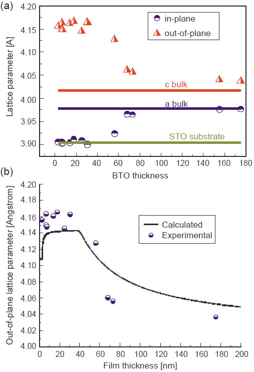
Figure 2: (a) Variation of the lattice parameters as a function of film thickness; (b) Calculated and measured thickness dependence of the polarization in epitaxial BTO films.
The maximum polarization Ps ≅ 43 μC/cm2 observed in our films is close to the values of 38.5 μC/cm2 and 44 μC/cm2 reported by Yanase et al. and Kim et al. for the same heterostructure. On the other hand, it is much smaller than the record polarization Ps ≅ 70 μC/cm2 measured in the 200-nm-thick BTO films grown on SrRuO3/DyScO3 [5]. The thickness dependence of Ps in our films at t ≤ 30 nm is qualitatively similar to the dependence reported in Ref. [2].
The coercive field was found to be relatively weakly dependent on the film thickness, being about 150 kV/cm.
In conclusion, our experimental study confirmed that the polarization and lattice strains in epitaxial BTO films may vary with the film thickness considerably. The maximum measured value of the out-of-plane lattice parameter is very close to the value predicted by the nonlinear thermodynamic theory. In contrast, the maximum measured polarization exceeds the theoretical value significantly (by about 23 %). The theoretical analysis demonstrates that the nonlinearity of the elastic properties alone cannot explain the discrepancy between the theory and experiment. Finally, we would like to note that reversible polarization may also increase in BTO films due to the presence of dipolar defects. Indeed, such defects were found to induce low-temperature ferroelectricity in (unstrained) thin films of STO, which is an incipient ferroelectric in the bulk form. However, the out-of-plane lattice parameter of these films at room temperature was significantly larger than the bulk lattice constant, probably because the dipolar defects involved oxygen vacancies. Hence it remains unclear whether the defect-induced additional increase of spontaneous polarization could be accompanied by a negligible lattice expansion. All in all, the origin of the polarization enhancement observed in epitaxial BTO thin films requires further experimental and theoretical investigations.
The financial support of Volkswagen-Stiftung within the program “Complex Materials: Cooperative Projects of the Natural, Engineering, and Biosciences” under the project I/77 737 entitled “Nano-sized ferroelectric Hybrids” is gratefully acknowledged.
- [1] Y. L. Li, L. E. Cross, L. Q. Chen, J. Appl. Phys. 98, 064101 (2005)
- [2] D. J. Kim, et al., Phys. Rev. Lett. 95, 237602 (2005).
- [3] A. Petraru, N. A. Pertsev, H. Kohlstedt, U. Poppe, R. Waser, A. Solbach, U. Klemradt, J. Appl. Phys. 101 (11), 114106 (2007)
- [4] J. Junquera, Ph. Ghosez, Nature (London) 422, 506 (2003)
- [5] K. J. Choi et al., Science 306, 1005 (2004)
A. Petraru, N. A. Pertsev, H. Kohlstedt, U. Poppe, A. Solbach1, U. Klemradt1, R. Waser
1II. Physikalisches Institut B, RWTH Aachen University, Germany
Double Beam Laser Interferometer – probing piezoelectric strain with sub-pm resolution
Task
Ferroelectric materials like lead titanate zirconate (Pb(Zrx,Ti1-x)O3) exhibit electromechanical properties besides their electrical properties used in ferroelectric random access memories (FERAM). In order to use these additional properties in micro-electromechanical systems (MEMS), e.g. actuators or sensors, different means of material characterization are needed. Several of the methods used in bulk material research, like charge integration under applied mechanical force and the resonance technique, are not suitable for thin film measurements. The former would cause additional charge transfer due to wafer bending and the latter approach is difficult due to the high frequencies needed (GHz range) for thin film geometries.
Approach
Instead, laser interferometry and scanning probe microscopy are used for this field of research, as both methods allow the nondestructive and within limits noninvasive characterization of ferroelectrics. The heterodyne double-beam laser interferometer setup (Figure 1) especially suited for thin film characterization, since this technique eliminates sample motions caused by bending.
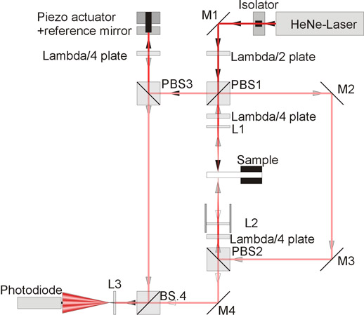
Figure 1: Optical Beam path of a typical double-beam laser interferometer. A darker beam color indicates two overlaying Beams. The patterned beam indicates interference of two beams. Lambda plates are used for polarization rotation and the isolator keeps reflected light from re-entering the stabilized beam source.
Instead, laser interferometry and scanning probe microscopy are used for this field of research, as both methods allow the nondestructive and within limits noninvasive characterization of ferroelectrics. The heterodyne double-beam laser interferometer setup (Figure 1) especially suited for thin film characterization, since this technique eliminates sample motions caused by bending. In combination with thermal, optical, vibration and air pressure insulation, it is possible to build an instrument capable of measuring the thickness change of a ferroelectric thin film under electrical field application with a sub-atomic resolution (<100 pm). Furthermore, no calibration measurement is needed, since the thickness change of the sample can be calculated directly from the photo detector response by:
ΔL = (Δ V λ) / (2 πVpp),
where ΔV is the amplitude of the detector response with active operating point stabilization, l is the wavelength of the laser, and Vpp is the interval between maximum and minimum detector response measured with deactivated stabilization. The interference pattern generated by an optimal aligned instrument is shown in Figure 2.
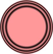
Figure 2: Interference pattern generated by to parallel laser beams und perfect alignment conditions. Center intensity at operating point is proportional to path length difference in both beams.
Results
In cooperation with the Ecole Polytechnique Fédérale de Lausanne (EPFL, Switzerland) and aixACCT Systems (Aachen), a double-beam laser interferometer was build during the cause of year 2001 (Figure 3). The instrument is seated on an air cushioned optical table positioned on ground level of the building and surrounded by a passive thermal chamber (Figure 4). Improvements were made in order to achieve shorter measurement times and easier alignment.
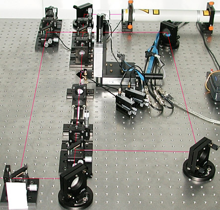
Figure 3: Close up view of the actual optical setup with indicated beam path. The beam exits on the lower left of the picture and is widened for intensity reduction and measurement of the center intensity.
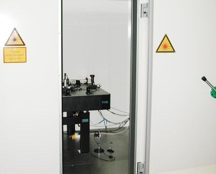
Figure 4: Thermal chamber surrounding the setup. The chamber is used for optical, thermal, acoustical and air pressure fluctuation insulation. Vibration insulation is achieved by active air cushioning of the optical table.
Using the lock-in measurement method used for short-time C/V measurements, it was possible to decrease the measurement time from several minutes to one second (∼1Hz). Additionally, the number of measurement points was increased from 200 to 5000. This method uses an external signal generator in combination with a simple operational amplifier circuit to superimpose the small signal generated by the lock-in over a relatively fast changing bias signal. Direct use of the internal lock-in oscillator helped to stay locked on the measured response and eliminated the need for a transmitted reference signal. Also, the electromechanical small-signal response could be acquired by and investigated with a digital oscilloscope. PC based measurement processing was only needed for calculation of the absolute values and data storage. At typical curve for PZT thin films near the morphotropic phase boundary (MPB) is shown in Figure 5. Furthermore, the lock-in method gives the ability to measure the electric small-signal characteristics of the sample without opening the chamber.
In order to measure the electromechanical large-signal response (butterfly curve, Figure 5, dotted line) at slow frequencies down to several Hz, the circuitry based feed back loop stabilization was replaced by a PC based solution with high time constants of several seconds. Such a method was only usable since the instrument is seated in noiseless environment and requires superior insulation. Both methods combined can be used to measure the electromechanical small- and large-signal characteristics of a material at the same time and with comparable parameters.
Additional improvements targeted electromechanical measurements on small capacitors down to 50 nm edge length. Using such small structures, two problems had to be solved. Firstly, the alignment of the beam reflection points on the samples front and back side had to be improved in order to measure the thickness change of the electromechanically active area. This was achieved by development of a new sample holder combining a defined, adjustable angle between beam and sample with a magnetic coupling. The latter was needed since the beam alignment was done with a special translucent sample. Hence, the DUT had to be exchangeable without readjusting the predetermined angle.
Secondly, the electric contacting point on the top electrode had to be moved away from the Laser reflection point in order to avoid beam distortions by the contacting needle. This was impossible to achieve for top electrodes smaller than 150 nm and standard layer geometry of the samples. Therefore, a special lithographic mask set was developed (Figure 6). The bottom electrode of the sample was etched to a striped layout and the ceramic layer was fabricated by standard chemical solution deposition (CSD) techniques. Afterwards, a dumbbell shaped top electrode was deposited on top of the ceramic layer. The part of the dumbbell with stripe of bottom electrode Pt underneath it is electrically active and the rest of the dumbbell is inactive. Hence, the active part could be used for optical measurements while the inactive part was used as extended contacting area.
By combination of all developments mentioned above it became possible to measure structures with an electrically active area down to 50 µm × 50 µm. Furthermore, the overhead time needed for instrument alignment and measurement was significantly reduced without sacrificing the resolution, which was measured to be 0.2 pm.
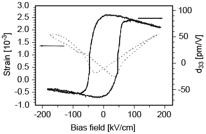
Figure 5: Electromechanical small-signal (black line) an d large-signal (dotted line) response of a PZT thin film with a composition near the morphotropic phase boundary. Both measurements were done simultaneously with comparable parameters. In contradiction to electrical measurements, the small-signal curve is hysteresis shaped while the large-signal response looks like an inverted C/V curve (butterfly-curve).
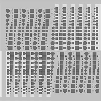
Figure 6: Mask layout for electromechanical measurements on small top electrode geometries (top right and bottom left corner). A striped bottom electrode is combined with dumbbell shaped top electrodes in order to separate the active capacitor area from the point of electrical contact.
P. Gerber, A. Roelofs, O. Lohse
Depolarizing-field-mediated 180° switching in PZT thin films
Task
The actual ferroelectric peculiarity, the reversibility of the spontaneous polarization make ferroelectric materials promising candidates for being used as storage media in future non-volatile memory devices. In the growing field of applications for ferroelectric thin films it is of great importance to understand the switching behavior of ferroelectric thin films in the nanoscale regime. Recent advances in the scanning force microscopy made it possible to image the nanoscale polarization reversal of ferroelectric films. A powerful tool to investigate and manipulate the domain structure is a modification of the scanning probe microscope (SPM) termed piezoresponse force microscope (PFM). A sketch of the PFM is shown in Figure 1. A phenomenological theory is used to explain the experimental observations.
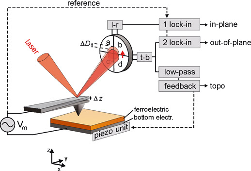
Figure 1: PFM setup to simultaneously acquire the topography and the in- and out-of-plane component of the polarization. A function generator is used to apply an alternating voltage Vw between the tip and the bottom electrode of the ferroelectric. The voltage induced cantilever deflection is detected by a reflected laser beam on a four sector photodiode.
Approach
Up to now, PFM was applied mainly for the detection of the polarization components normal to the film surface. Recently, it was shown that this technique enables the observation of in-plane polarization as well. Here we report PFM investigations of the polarization switching in epitaxial PbZr0.2Ti0.8O3 (PZT) thin films containing multiple 90° domains (twins). Changes of both out-of-plane and in-plane polarizations in the film are monitored during the field-induced switching and subsequent relaxation. During scanning a ferroelectric or piezoelectric thin film an alternating voltage is applied through a conducting cantilever. Due to the inverse piezoelectric-effect the thin film is locally deformed. The deformation of the ferroelectric thin film and the orientation of the polarization are linked by the piezo-coefficients (see Figure 2). The ferroelectric heterostructure used in this study consisted of a 400-nm-thick PZT film epitaxially grown on a [001] single crystalline SrTiO3 (STO) substrate with an intermediate 50-nm-thick La0.5Sr0.5CoO3 (LSCO) oxide layer employed as the bottom electrode. At room temperature, as-grown PZT films displayed the presence of a two-dimensional grid of 90°domains (a domains) embedded into the ferroelectric matrix with the tetragonal c axis being oriented orthogonal to the substrate (c domain).
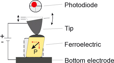
Figure 2: Converse piezoelectric effect in ferroelectric grains investigated by PFM. The applied electric field leads to a lifting of the cantilever due to the d33 (out-of-plane-signal) and additionally causes the d15 a shear movement which leads to a torsion of the cantilever (in-plane-signal).
Results
The inspection of the piezoresponse images shows that the observed configuration is always of the “head-to-tail” type (Figure 3). The native c– domains were switched by 180° into c+ domains by applying a negative voltage of –8 V to the conductive cantilever and ground to the bottom electrode while scanning a square pattern of approximately 4 × 4 µm2. From the piezoresponse image shown in Figure 3(c) we see that the poled c– domains transformed almost completely into the c+ ones. Moreover, the in-plane polarization in most parts of the a domains was observed to switch by 180° as well [see Figure 3(d)], though the electric field is applied mainly in the film-thickness direction. It can be seen that the polarization configuration gradually relaxes back to the initial state. Several needle-like c– domains appear near 90° walls and then grow laterally in the film plane, as shown by circles in the inset in Figure 2(c).
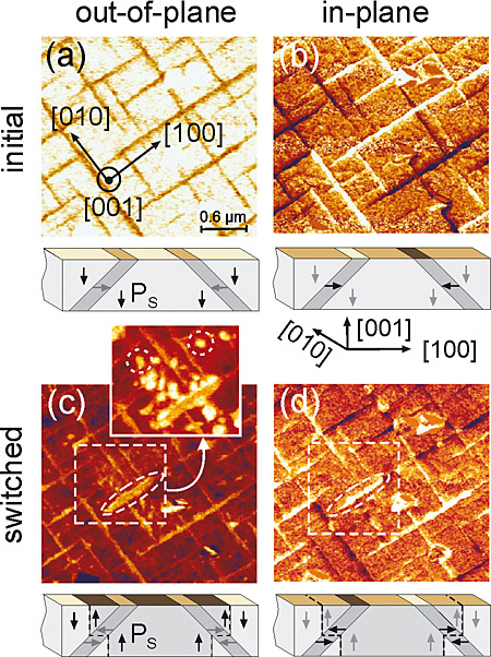
Figure 3: Piezoresponse images of an epitaxial poly-domain PZT thin film in the as grown state, (a) out-of-plane image, (b) in-plane image and after poling (c), (d). Regions with bright, dark, and intermediate contrast correspond to different domains, as shown schematically in the sketches below the PFM images. The inset in (c) shows the region from where the back-switching starts. Circled areas in the inset indicate reversed needle-like 180° domains near 90° walls.
It is known that the spontaneous polarization and equilibrium domain structure of epitaxial ferroelectric thin films should strongly depend on the misfit strain Sm between the film and substrate. The misfit strain at room temperature can be evaluated as Sm ≈ (ab – a0) (T – Tg), where ab and a0 are the linear thermal expansion coefficients (TECs) of the substrate and the film prototypic cubic phase, respectively. Taking for the TECs of STO and PZT 20/80 the average values of ab × 11 × 10–6–K–1 and a0 × 6 × 10–6 K–1,15 we obtain Sm × –3 × 10⁻³. Evaluating the depolarizing field inside the plate-like a domains having “head-to-head” or “tail-to-tail” polarization configurations relative to adjacent c ones show that a domains at room temperature should be uniformly polarized and are not expected to contain 180° domain walls. In the linear approxmation, the in-plane component E of the electric field is given by using the calculated value of PaS = 0.67 C/ma2 and assuming (ec + ea)/2 to be about 300 or less, we obtain × 250 MV/m. Since this intensity is much larger than the measured coercive field Ec ∼ 10 MV/m of the investigated PZT films, the “head-to-head” or “tail-to-tail” polarization configurations of embedded a domains are definitely unstable. This result explains why only “head-to-tail” configurations were observed in PZT films even though the switching field was applied manly in the film-thickness direction.
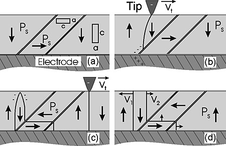
Figure 4: The expected scenario of polarization switching and relaxation in polydomain PZT films: a) initial c/a/c domain state with the native downward polarization in the c - domains; b) imaginary transient domain configuration during the tip-induced local 180° switching; c) forward growth of the residual c - domain after the removal of the applied field; d) lateral motion of the 180° domain boundaries during the second stage of back-switching.
A. Roelofs