Simulation and Modelling
Modelling on different scales and with a variety of approaches are performed for phenomena, materials, and devices. Model-based numerical simulations are employed using both, self-developed program modules and commercial standard tools. The approaches comprise Finite Element/Difference Methods (FEM / FDM), Monte Carlo (MC) and Molecular Dynamics (MD) methods, as well as analytical calculations based on the band theory, the thermodynamics, and drift-diffusion transport theory. For example, we model the point defect disorder in oxides, electrostatic and electromagnetic fields by FEM/FDM, electron injection and transport on the microscopic scale of single molecules and on the macroscopic scale for metal-insulator-metal systems, redox processes and electrochemical metallization by MD methods. We cooperate closely with theory institutes in order to link our micro- and nanoscale simulation to ab-initio quantum mechanical models in which, e. g. local electron densities in crystal dislocation can be calculated on the atomic scale.
Numerical Simulation and Modeling – an Overview
Short Description
Simulations on different scales and using a variety of approaches are performed for both basic materials and complex devices. Our simulation and modeling activities cover simulation of physical mechanisms as well as layout and analysis of electrical circuits.
Physical Modeling and Simulation
We conduct finite element (FEM) and finite difference (FDM) simulations to phenomenologically investigate physical mechanisms in materials and devices up to 3D. For these simulations we use both commercial software packages (COMSOL Multiphysics, CST Microwave Studio) and self-developed program packages.
- Electro-thermal coupling
- Electrochemical simulations
- Drift-diffusion problems
- Quasi-static to radio frequency electrical simulation
- Piezoelectric-mechanical coupling
Atomistic simulation techniques are employed to examine the effects of crystal defects and ion migration at microscopic level (Software GULP as well as self-developed code).
- Energy minimization (molecular statics) in crystals
- Molecular dynamics using a force field
Circuit Layout and Simulation
- Layout tool for printed circuit boards (Altium Designer)
- Simulation tools for dc up to RF (Software Spice)
EXAMPLES
Physical Modeling of Resistive RAMs (ReRAMs) Based on Electro-Chemical Mechanisms (ECM and VCM Cells)
Growth of filaments in an ECM cell
We simulated filamentary growth during the SET operation in an electrochemical metallization (ECM) cell with two different seeds using a 2D finite element model. A 40 ns triangular current sweep is used as stimulus. As soon as the right filament approaches half of the length to the counter electrode, the growth speed of the left filament slows down and it finally stops growing. This demonstrates that only one filament is responsible for the SET operation. The simulation is conducted using COMSOL Multiphysics.
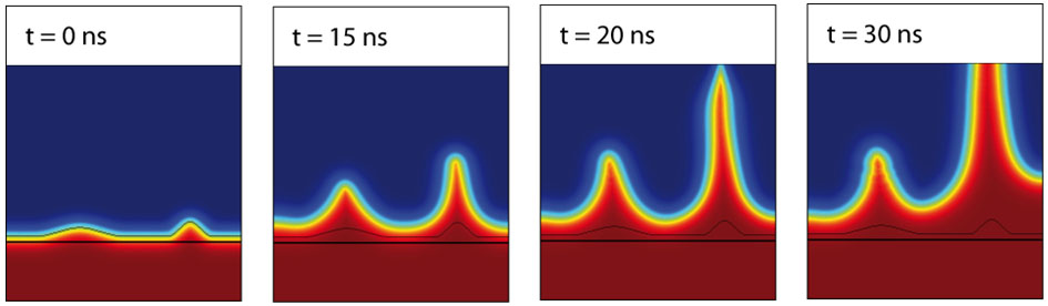
Figure 1: 2D FEM simulation of the filamentary growth during SET operation in an ECM cell with two seeds.
Formation of a chemical polarization in VCM cells
During electroforming of valence-change memory (VCM) cells, conducting regions are created in the oxide material due to redistribution of the oxygen vacancies. These regions – often referred to as the virtual cathode – propagate towards the active electrode. To gain a better insight into the forming process, we calculate static current density-voltage characteristics of metal-insulator-metal structures with a Schottky-like interface and an ohmic interface assuming different oxygen vacancy distributions.
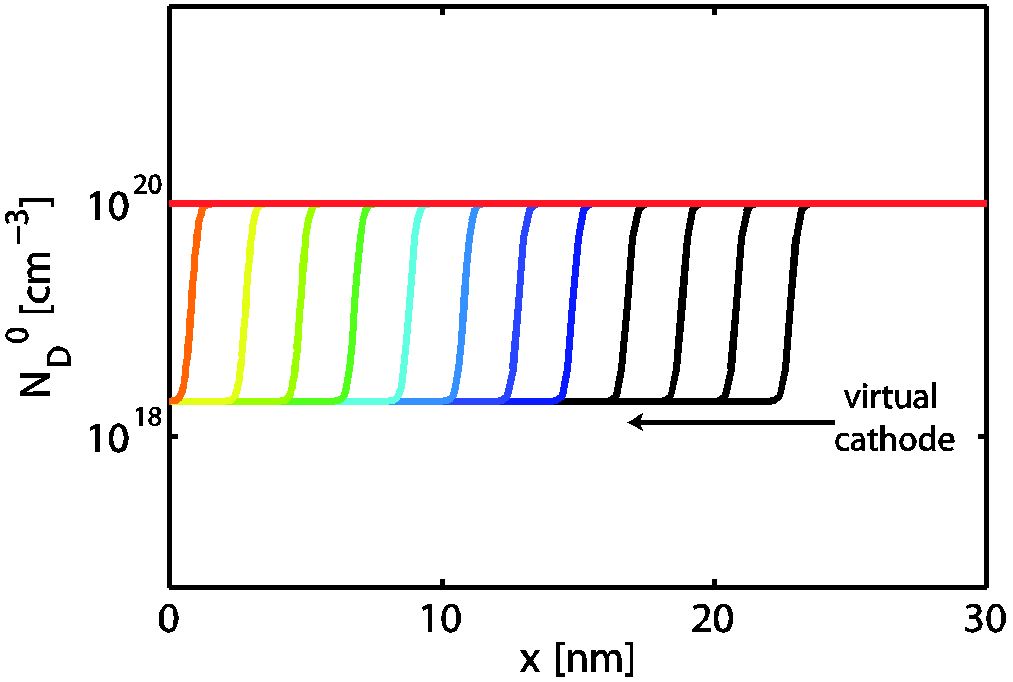
Figure 2: Different dopant profiles emulating the propagation of the virtual cathode
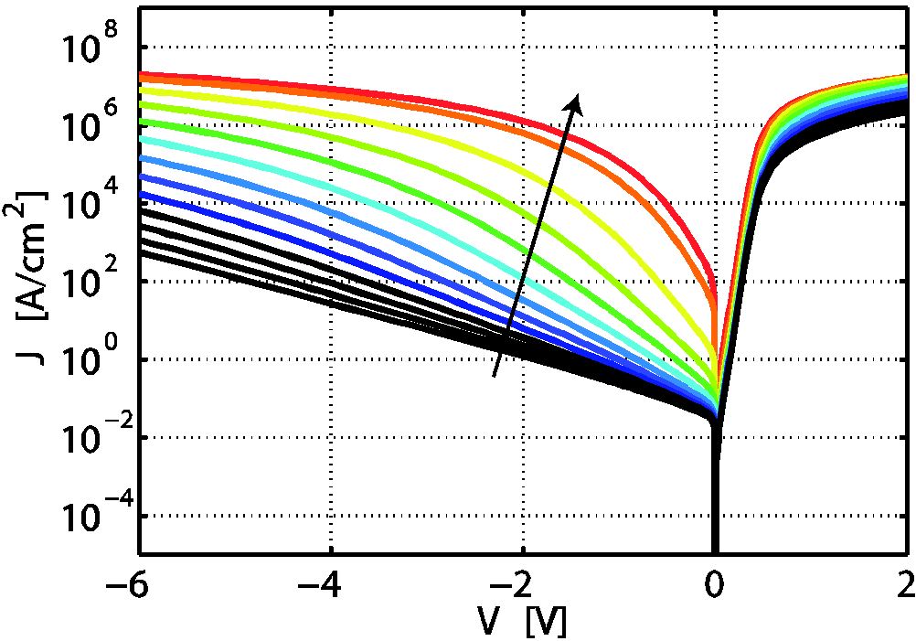
Figure 3: Resulting J-V characteristics.
Molecular dynamics simulations of oxygen vacancy diffusion in SrTiO3
Classical molecular dynamics simulations were conducted to examine the diffusion characteristics of oxygen vacancies in the model material strontium titanate. Both, the bulk diffusion and diffusion near a Σ3(111) grain boundary were investigated. We used additional static simulations to ensure the reliability of the potential model and to calculate the vacancy-vacancy interaction in different configurations.
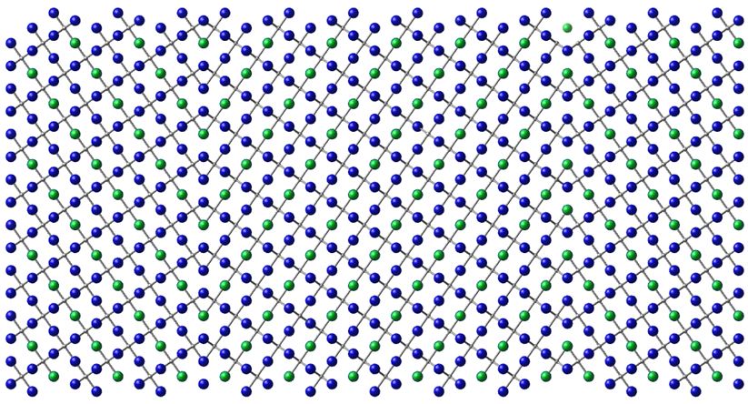
Figure 4: Simulation cell of SrTiO3 with two Σ3(111) grain boundaries including 8160 ions (blue: oxygen, green: strontium, grey: titanium).
Molecular dynamics simulation of dendrite growth in an ECM cell
We used a molecular dynamics to simulate the Brownian motion of copper ions in an applied electric field. The interactions between different copper ions are modeled using suitable potentials. In addition the attraction of the negatively charged dendrite and the copper ions is taken into account. This simulation results in a dendrite growth as shown in Figure 5.
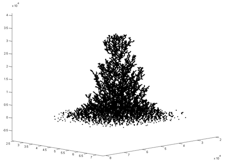
Figure 5: Dendrite growth in ECM cells.
Dynamic Simulation of Memory Cells with SpiceOpus
Resistive switches can be modeled in terms of memristive systems to simulate the dynamic device behavior. More complex structures like crossbar arrays can be simulated with these device models.
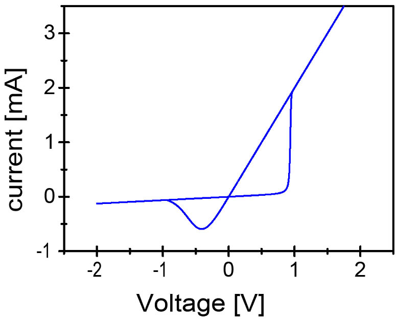
Figure 6: I-V characteristic of an ECM cell modeled as memristive system.
Physical Modeling of Microelectro-Mechanical Systems (MEMS) Based on Ferroelectric Materials
FEM simulations (COMSOL) are performed to design and optimize piezoelectric microsystems for vibration-based energy harvesting concepts.
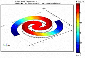
Figure 7: FEM-Simulation of Spiral-Shaped Cantilever Beam. Color-coded is the displacement.
RF Simulation of Tunable Devices (Phase Shifters etc.) with Varactors and MEMS
One difficulty in designing tunable filters is to avoid variations of bandwidth in dependence of the tuning state. The filter is optimized in simulations using CST Microwave Studio so that the bandwidth remains constant when tuning the center frequency by altering the varactor capacitance.
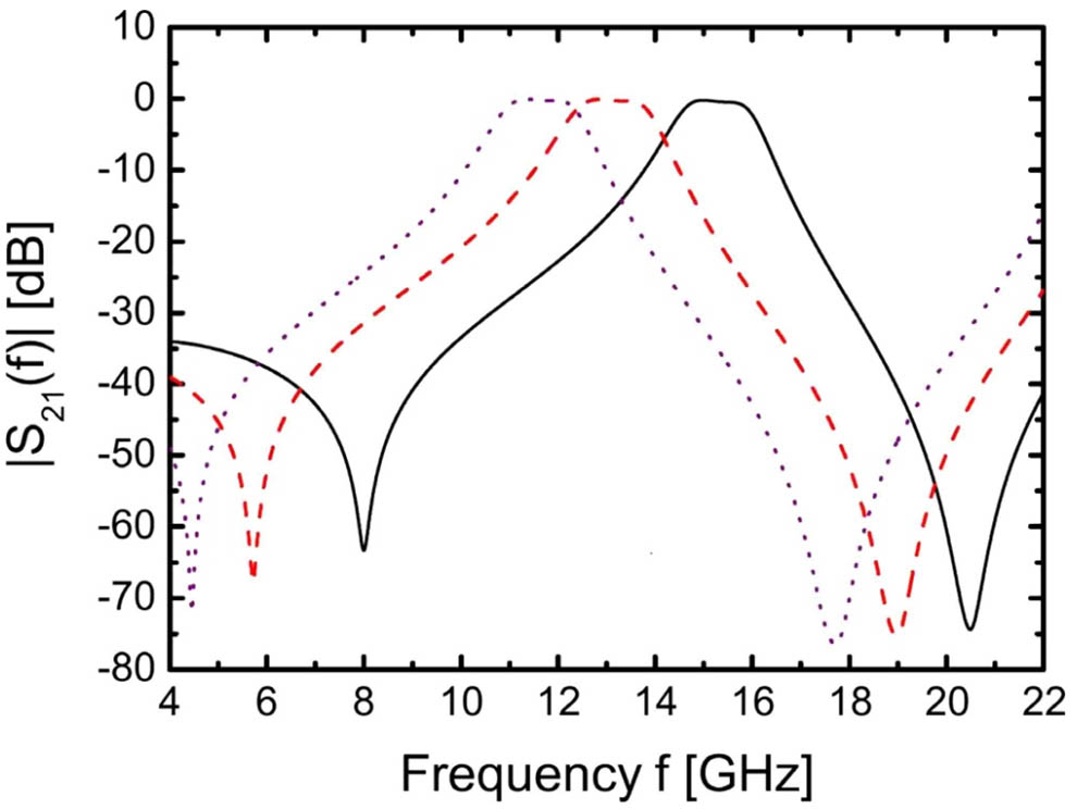
Figure 8: Simulated transfer characteristics of a tunable bandpass filter using ferroelectic varactors at high GHz frequencies.
Simulation and Layout of Operational Amplifier Circuits for Measurement Applications
Measurement of different physical quantities requires specific adapted measurement circuits to reach the requested goal, e.g. high resolution or high speed measurements. Altium Designer is used for development and simulation of measurement circuits. Shown below is a transimpedance amplifier for current to voltage conversion used in measurements of electrochemical cells.
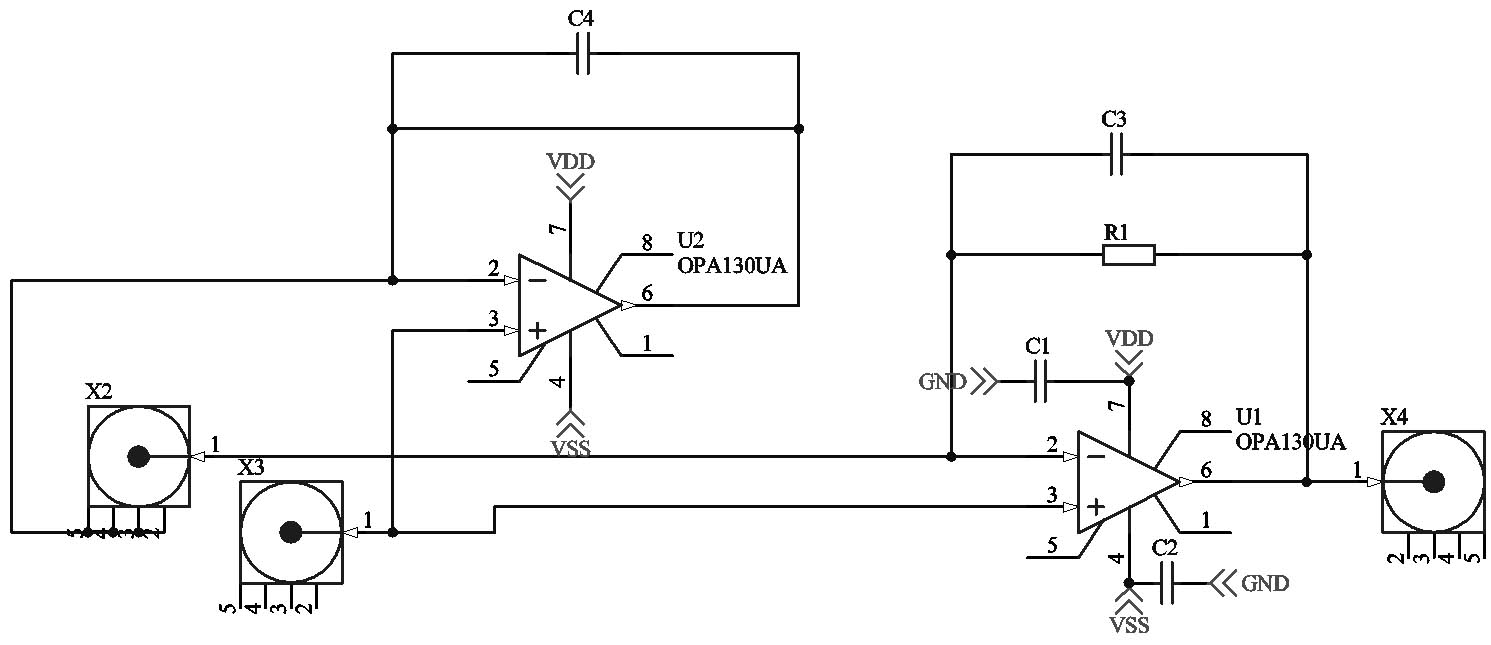
Figure 9: Transimpedance amplifier for current to voltage conversion.
A. Marchewka, S. Menzel, A. Hennings, E. Linn, A. Burkert, M. Röscher
Molecular dynamics simulations of oxygen vacancy diffusion in SrTiO3
TASK
Detailed understanding of the basic physical and chemical mechanisms in oxide-based resistive switching materials is still lacking. A theoretical approach on the atomic level needs to be able to describe systems of several thousand atoms in dynamical nanosecond-long simulations to be comparable to experimental switching events and timescales.
APPROACH
A classical force-field model with partial ionic charges was applied to study the behaviour of oxygen vacancies in the perovskite oxide strontium titanate (SrTiO3). The dynamical behaviour of these point defects was investigated as a function of temperature and defect concentration by means of molecular dynamics (MD) simulations. The interaction between oxygen vacancies and an extended defect, here a Σ3(111) grain boundary, was also examined by MD simulations. Analysis of the vacancy distribution revealed considerable accumulation of vacancies in the envelope of the grain boundary. Possible clustering of oxygen vacancies in bulk SrTiO3 was studied by static lattice calculations within the Mott-Littleton approach. All binary vacancy-vacancy configurations were found to be energetically unfavourable.
RESULTS
We conducted molecular dynamics simulations with supercells of oxygen deficient strontium titanate at different temperatures for 1 ns in each case. The diffusion coefficients was calculated for oxygen vacancies and compared to literature data as can be seen in Figure 1. Due to computational limitations the concentration of oxygen vacancies is considerably higher than experimental concentrations. In this case the vacancies are not moving interaction-free and the diffusion coefficient is lowered by about one of magnitude compared to the literature values. However, the calculated activation energy of ΔH = 0.93 eV agrees very well with literature data.
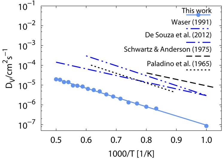
Figure 1: Simulated temperature dependency of the oxygen vacancy diffusion coefficient in STO. The slope reveals an activation enthalpy of ΔH = 0.93 eV.
The diffusion of oxygen vacancies near two Σ3(111) grain boundaries was investigated by introducing an initial distribution of vacancies near one of the two grain boundaries. The comparison of initial and final distribution after 1 ns MD simulation at 1000 K in Figure 2 indicates the tendency of vacancies to accumulate at the grain boundary.
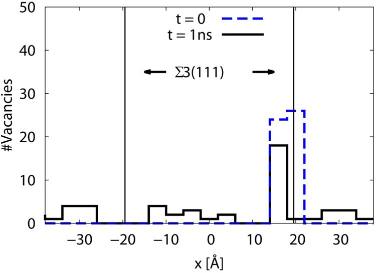
Figure 2: Initial and final distribution of oxygen vacancies near two Σ3(111) grain boundaries.
The MD simulations were supported by lattice dynamics simulation of the interaction of two oxygen vacancies in the Mott-Littleton approach. As seen in Figure 3 the interaction energy is positive/repulsive in general and extends to distances larger than that of nearest neighbours. Linear chains of vacancies along Ti-O-Ti-O chains are energetically unfavourable.
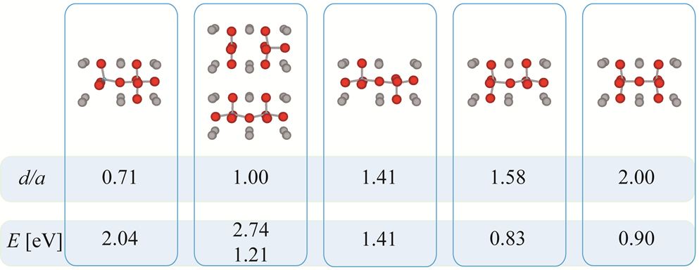
Figure 3: Interaction energy of two oxygen vacancies in different configurations.
M. Schie, A. Marchewka, T. Müller, R. A. De Souza and R. Waser
J. Phys.: Condens. Matter 24 (2012) 485002 doi:10.1088/0953-8984/24/48/485002
Simulation of the switching mechanism in metal ion migration-based resistively switching model systems
Coplanar structures offer the opportunity to investigate resistive switching in metal ion migration-based memory cells. A Pt/H2O/Ag cell is utilized here as a model system, due to its simplicity and the feasibility of visual inspection of the switching process. Bipolar switching is achieved for the cell, and a current jump of about 5 orders of magnitude is measured upon switching-on. Scanning electron microscopy (SEM) investigations demonstrate that the growth and dissolution of Ag dendrites are responsible for the resistive switching. The switching characteristics are simulated and the Ag dendrite morphology is proposed to be the origin of the asymmetrical dissolution during the switching-off process.
Electrochemical metallization memory cells are based on metallic filament formation and rupture in an insulating material sandwiched between an oxidizable and an inert electrode. Ge0.3Se0.7 [1] as well as SiO2 [2] can be used as insulating matrix in which filament growth occurs. While the switching-on process is understood quite well, a few general questions remain open for the switching-off process. In particular, how and where the rupture of metallic filaments is carried out is still unclear. When a high enough current is driven through the system, metallic filaments can definitely be ruptured by Joule heating. Two questions have to be dealt with: what causes the filament rupture in the low-current regime, and what causes the bipolar I-V characteristics, despite of the chemical symmetry in the cell after switching-on?
To facilitate the observation of the switching processes, a coplanar structure, instead of the common metal-insulator-metal stack structure, was fabricated on SiO2 substrates by photolithography [3]. Cells consisting of an oxidizable Ag electrode, de-ionized water and an inert Pt electrode were prepared as model systems for the electrochemical metallization cells (Figure 1 (a)). The gaps between the Pt electrode and the Ag electrode were in the range of 0.6 to 100 μm. Figure 1 (b) shows the bipolar hysteretic resistance-voltage characteristics of a cell with a Pt/Ag gap of 0.65 μm. The cell was switched on at ∼−0.28 V with a current jump of ∼5 orders of magnitude, and switched off at ∼0.37 V. Owing to the 1 mA current compliance, the relatively large heat capacity and convection of water, the effect of the Joule heat can be excluded.
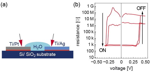
Figure 1: (a) Cell structure, and (b) characteristic R-V curve. For electrical characterization the Pt electrode was grounded.
The switching-on process is illustrated in Figure 2. After applying −1 V to a Pt/H2O/Ag cell with a Pt/Ag gap of 3 μm for about 4 s, the cell was switched on (Figure 2(a)). Therefore, −1 V was applied to cells of the same structure for 1, 2 and 4 s, respectively, and the cells were investigated by Scanning Electron Microscopy (SEM) afterwards. According to Figs. 2(b) to (d), metallic dendrites grew from the Pt electrode toward the Ag electrode.
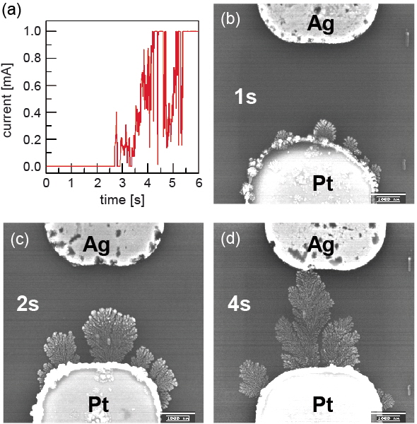
Figure 2: The switching-on process while applying −1 V to a Pt/H2O/Ag cell with a Pt/Ag gap of 3.0 m: (a) I-t curve, (b), (c) and (d) SEM images, showing the Ag dendrite growth after applying −1 V for about 1, 2 and 4 s, respectively.
The switching-on process consists of the following steps: (1) metallic Ag is electrochemically oxidized to Ag+ ions at the Ag electrode/H2O interface according to the reaction Ag → Ag+ + e′, (2) Ag+ ions migrate through H2O to the Pt electrode due to the electrochemical potential difference between the Ag and the Pt electrode, (3) at the Pt electrode/H2O interface, Ag+ ions are reduced back to metallic Ag according to the reaction Ag+ + e′ → Ag. As a consequence, metallic Ag dendrites grow from the Pt electrode toward the Ag electrode.
The dendrite morphology is fractal. The situation immediately before the dendrite front contacts the Ag electrode is sketched in Figure 3(a). After switching-on, the cell becomes Pt/Ag dendrite (H2O)/Ag, with a metallic Ag bridge, as shown in Figure 3(b). We assume that the contact point is only a few atoms wide, because such a contact is sufficient to establish the low resistance state and to activate the current compliance. The originally asymmetric Pt/H2O/Ag cell becomes chemically symmetric, because two Ag electrodes are involved at the microscopic level. However, the cell actually remains asymmetric in a morphological sense. On the microscopic level, the contacting twig and the approximately planar Ag counter electrode are extremely different in their curvatures. On a macroscopic level, this corresponds to a huge difference in volume density between the Ag dendrite and the solid Ag electrode.
Upon applying a positive voltage to the Pt electrode, a switching-off process sets-in: In parallel to the electronic current across the Ag twig, the positive voltage drop activates the oxidation reaction, Ag → Ag+ + e′, on all dendrite surfaces with a positive potential, while the electrochemical reduction and deposition takes place on the Ag electrode surface with a negative potential. A numerical field simulation using the software COMSOL™ was used to determine the equal potential lines and the field vectors in the vicinity of the twig. As shown in Figure 3(b), the major voltage drop is located at the neck where the twig touches the planar Ag electrode. This leads to dissolution of the bridge very near the neck position. Because of the tiny volume of the twig, a significant length of the dendrite is easily dissolved, while the re-deposition takes place at the solid Ag electrode, so that the geometric front of the electrode only moves insignificantly towards the rapidly retreating dendrite front (Figure 3(c)). As a result, the gap between the Ag electrode and the Ag dendrite increases, and the cell is switched off. Despite of its symmetric chemical nature, the geometric asymmetry of the cell allowed for repetitive switching in the following.
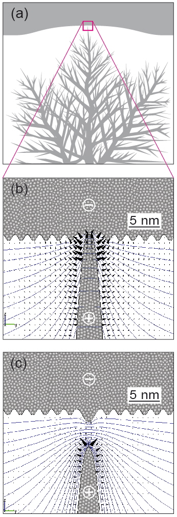
Figure 3: Field simulation results of the front-most Ag dendrite and the Ag electrode: (a) Sketch of the Ag dendrite and the solid Ag electrode in contact. (b) Tip of the Ag dendrite in higher magnification during the late ON-state. The blue lines represent equal potential lines after applying an switching-off voltage of 200 mV. The voltage difference between two adjacent lines is 10 mV. The black cones represent the electrical field and point to the direction of the Ag+ ion migration. (c) Early OFF-state. As soon as the electronic contact is disconnected, the field distribution changes, which accelerates the further dissolution of the dendrite tip.
In conclusion, bipolar resistive switching was reproduced for Pt/H2O/Ag model cells. The switching-on process is based on Ag dendrite formation bridging the gap between the Pt electrode and the Ag counter electrode. The switching-off process sets in when the voltage is reversed. It starts by the electrochemical dissolution of Ag atoms in the contacting dendrite. A numerical simulation shows that the dissolution starts at the neck where the dendrite contacts the solid surface, leading to a fast retreating of the dendrite. On the microscopic scale, the tremendous curvature difference between the dendrite and the planar Ag bulk constitutes the reason for the bipolar switching of the cell.
- [1] C. Schindler, K. Szot, S. Karthäuser, and R. Waser pss RRL 2, 129-131 (2008).
- [2] C. Schindler, M. Weides, M.N. Kozicki, and R. Waser Appl. Phys. Lett. 92, 122910-1-3 (2008).
- [3] X. Guo, C. Schindler, S. Menzel, and R. Waser Appl. Phys. Lett. 91, 133513-1-3 (2007).
Institut für Festkörperforschung - 6, Forschungszentrum Jülich GmbH, and Jülich-Aachen Research Alliance, Section Future Information Technologies (JARA-FIT), 52425 Jülich, Germany, contact: r.waser@fz-juelich.de
Simulation of Multilevel Switching in Electrochemical Memory Cells
A simulation model for bipolar resistive switching in electrochemical metallization memory cells is presented. The model is based on an electrochemical driven growth and dissolution of a metallic filament. The origin of the multilevel switching is proposed to be a direct tunnelling between the growing filament and the counter electrode. The model fully reproduces the experimental data and allows for an explanation of the transition from bipolar to unipolar switching.
Electrochemical metallization memory (ECM) cells are a promising candidate for next generation non-volatile, high speed and highly scalable memory cells [1,2]. The switching is attributed to the electrochemical growth and dissolution of a Cu or Ag nano-sized filament. Typically, ECM cells consist of a Cu or Ag active electrode, an ion conducting switching layer (SL) and an inert electrode. During the SET process a positive potential is applied to the active electrode which is oxidized. Ag or Cu cations are driven out of the active electrode and migrate through the switching layer. At the inert cathode the cations are reduced and a metallic filament grows towards the anode resulting in a low resistive state (LRS). To RESET the device to a high resistive state (HRS), the voltage polarity is reversed and the filament dissolves. Based on this switching mechanism we developed a dynamic simulation model for multilevel switching in ECM cells [3]. The origin of multilevel switching is proposed to be direct tunneling between the growing filament and the active electrode. It is shown that the different low resistive states (LRS) are achieved by modulation of the corresponding tunneling gap. The nonlinear switching kinetics is modeled by the electron transfer reaction, which occurs at the electrode/ insulator interfaces.
Figure 1 shows a schematic of the simulation model. The metallic cylindrical filament growth from the inert bottom electrode through the SL and modulates the tunneling gap x. Within the SL ionic and electronic tunneling currents are present. The ionic current path is modeled by two voltage controlled current sources (ηac, ηfil), which represent the electron-transfer reactions at the boundaries (see explanation below), and the resistance due to ionic drift Rion(x). The electronic current path is attributed to electronic tunneling, represented by one voltage controlled current source VTu. The LRS is reached as the tunneling gap is small enough to enable significant tunneling current.
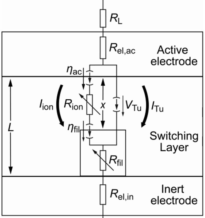
Figure 1: Schematic of the switching model with equivalent circuit diagram. The switching layer of thickness L is sandwiched between the active top electrode and the inert bottom electrode. A cylindrical filament growth within the SL and modulates the tunneling gap x between filament and active electrode. The elements of the equivalent circuit are an optional load resistor RL, the electrode resistors Rel,ac and Rel,in and the filament resistor Rfil(x).(Redrawn from [3])
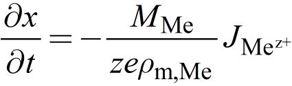
The filament growth/dissolution and thus the change of x can be described using Faradays law
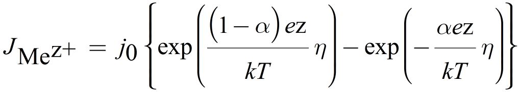
Here, JMez+ is the ionic current, z the charge transfer number, MMe the atomic mass and ρm,Me the mass density of deposited metal. The redox reactions at the electrodes involve an electron transfer reaction. The resulting current density due to this charge transfer is described by the Butler-Volmer equation and defines the ionic current
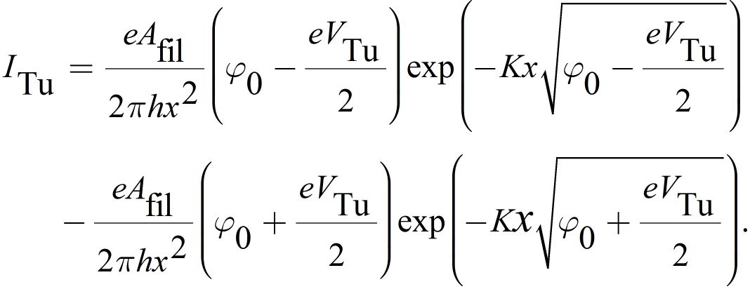
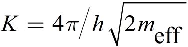
Here j0 is the exchange current density, α the charge transfer coefficient and η the overpotential. The tunneling current ITu can be calculated according to Simmons as
where
Due to the exponential dependence of ITu on x, the LRS is very sensitive to small variations in x. For small voltages VTu the tunnel junction shows an ohmic behavior, which is consistent with the experimentally observed characteristic of LRS in ECM cells. Using Kirchhoffs laws a implicit equation for the filamentary overpotential can be obtained and the equation system can be solved.
Figure 2: (a) Simulated I-V curve (red) and corresponding relation between Vcell and Vapplied (blue). (b) Experimental I-V characteristic for a Cu/SiO2/Pt cel.l (Redrawn from [3]).
As a model system for the simulations a cylindrical Cu/SL/Pt structure is used. Both electrodes have a thickness of 20 nm and a 100 nm radius, which leads to an electrode resistance Rel = 76 mΩ. RL is zero in all simulations. The SL thickness is L = 20 nm. Due to numerical simplicity we set Aion = Aac = Afil = π rfil2. Further parameters are z = 2, ρm,Cu = 8.95 g/cm3, MCu = 1.06⋅10-22 g and T = 300 K. As reference material in the simulations we choose SiO2 and thus φ0Cu/SiO2 = 4.2 eV and mr,SiO2 = 0.86. The remaining reference values are ρion = 10-2 Ωm, j0 = 10-2 A/m2 and rfil = 2 nm. Figure 2(a) shows the simulated I-V characteristic (red solid line) using a current compliance of 10 μA. The ECM cell is initially in HRS. As excitation a triangular voltage with 1 V amplitude and 1 s rise time is used in all simulations. During SET operation the actual cell voltage is not equal to the applied voltage (cf. blue curve in Figure 2(a)). As soon as the set ISET is reached, Vcell first drops abruptly. Afterwards it decreases gradually during the current control. The simulation results are in good agreement to experimental data shown in Figure 2(b).
In order to study the multilevel programming we performed simulations with varying set current ISET. The simulated LRS values are shown in Figure 3(a) along with experimental data. Evidently, the proposed tunneling model is capable of explaining multilevel switching over the full range of SET currents. The remaining gap xmin is proportional to log(ISET) = −1 and changes from 1.10 nm at 1 pA to 0.13 nm at 398 μA. At higher SET currents the gap is closed completely resulting in a metallic contact. Also for the relation between RESET and SET current experimental data and simulation data are consistent (cf. Figure 3(b)).
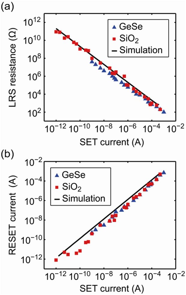
Figure 3: (a) LRS resistance vs. SET current and (b) corresponding RESET current vs. SET current. The simulation results for (a) and (b) are depicted as black solid lines. Experimental data is displayed as blue triangles for a Ag:GeSe system [4] and as red squares for a Cu:SiO2 system.[4] The filament radius is rfil = 8 nm.(Rredrawn from [3])
In conclusion, we presented a physical simulation model for resistive switching in ECM cells. We proposed tunneling as the origin of multilevel switching rather than filament diameter variation, whereas the LRS level is controlled by ISET. A metallic contact is still possible for a high ISET. This allows for an explanation of the transition from bipolar to nonpolar switching. The former occurs as long as a tunneling gap remains, whereas nonpolar switching occurs for a metallic contact. Its dissolution might involve Joule heating and thus allows for a nonpolar RESET.
- [1] R. Waser, M. Aono, Nat. Mater., 6 (2007) 833.
- [2] I. Valov, R. Waser, J. R. Jameson, M. N. Kozicki, Nanotechnology, 22 (2011) 254003/1.
- [3] S. Menzel, U. Böttger, R. Waser, J. Appl. Phys., 111 (2012) 014501.
- [4] C. Schindler, PhD thesis, RWTH Aachen, vol., pp., 2009.
S.Menzel, U. Böttger, R. Waser
A Novel Reference Scheme for Reading Passive Resistive Crossbar Memories
A great effort today is concentrated on the development of resistive hysteretic materials and their related memory architecture. Resistive memories have a promising future to replace all current memory technologies to present an all-in-one memory solution. Passive resistive memories are of a special importance since they can be scaled into the nanometer range without losing their functionality. This work is concerned with a novel scheme for generating reference voltages for the read operation. The scheme can be used with any passive crossbar based memory, regardless of the materials used for the implementation of the memory elements.
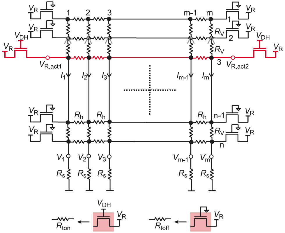
Figure 1: Real crossbar array with row access transistors and sense resistors.
A crossbar resistive memory consists of vertical and horizontal conductive lines with a hysteretic resistive material separating them at the cross points. In a real crossbar, the resistances of the interconnects, the sensing elements, and the voltage source/s required for the read operation are considered as shown in Figure 1.
To realize the read operation, voltage is applied to the rows using NMOS row access transistors which have an equivalent on-resistance Rton when switched on and an equivalent off-resistance Rtoff when switched off. Rton and Rtoff are considered to have values in the order 103 Ω and 107 Ω respectively [1].
Due to the voltage drops at the interconnects, the sensing elements and since the non-accessed cells are not isolated, parasitic currents will flow through the memory cells in the non-accessed rows. In addition, the resistance of the row access transistors will reduce the actual read voltage VRact applied to the row because they construct a voltage divider with the equivalent resistance of the rows.
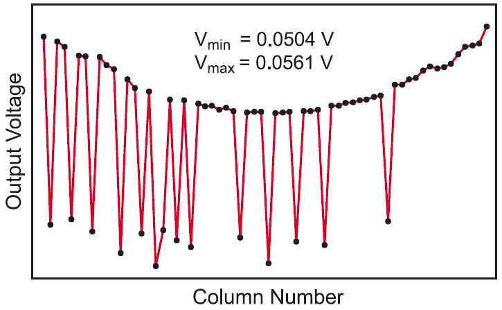
Figure 2: Simulation result of a row from a 64 × 16 crossbar array considering the parasitic elements and a 0.8 probability of the “1”s.
The non-accessed rows are left open which means that the row access transistors are turned off and have an equivalent resistance of Rtoff. To reduce the voltage degradation, voltage is applied from both sides of the array. The output voltages resulting from reading a row of a 64 × 16 bit array are shown in Figure 2.
The simulation parameters are VR = 1 V, Ron = 10 kΩ, Roff = 40 kΩ, Rh = 10 Ω, Rv = 10 Ω, Rton = 5 kΩ, Rtoff = 10 MΩ, and Rs = 10 kΩ. Ron and Roff are the resistances of the memory cell element in the “on” and “off” states respectively. Rh and Rv are the resistances of the horizontal and vertical interconnects between two adjacent cells respectively. The last parameter Rs is the value of the sense resistor. The pattern stored in the array is a random pattern with 0.8 probability of the “1”s.
It is obvious from the previous simulation that the output voltage levels are degraded when the parasitic resistances of the different memory elements are considered. Thus, it is not possible to use a constant reference voltage to differentiate between a “1” and a “0” especially if we considered that the voltage levels will change by changing the stored pattern. Since the degradation is severer for larger arrays, it will be a limiting factor for the maximum obtainable array size. Thus, an alternative method for generating a reliable reference voltage is required.
The cells in one row are locally strongly correlated regardless of the values of the sense resistors, parasitic resistances of the different elements, or the stored pattern. This locality can be utilized to generate a reference voltage by dedicating some cells from each row to act as reference cells [2].
In this new reference scheme every two horizontally adjacent reference cells generate a local reference voltage for the cells between them as can be seen in Figure 3. The number of the reference cells is determined depending on the grade of degradation of the output voltages. Higher voltage degradation will require more reference cells.
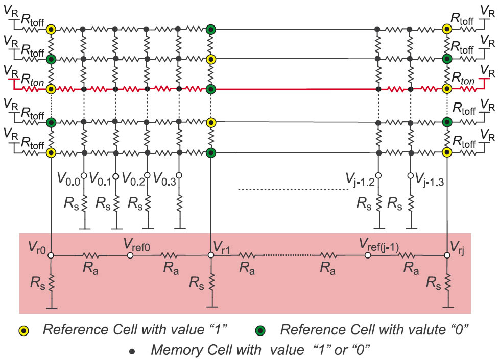
Figure 3: The crossbar array after inserting reference cells and reference generating capacitors or resistors.
The values stored in the reference cells in a row are “1” and “0” (low and high ohmic) alternately. The first and last cells in a row are always reference cells. The horizontal position of the reference cells is identical in all rows, which constructs columns of reference cells (reference columns). Vertically adjacent reference cells have also values of “0” and a “1” alternately. Reference cells are physically the same as normal memory cells; however they are preprogrammed with constant values to generate reference voltages.
An ideal reference voltage would be the average value of the “1” and “0” voltage levels. To generate the local reference voltages, every two adjacent reference columns are connected together using two identical resistors (Ra) as can be seen in Figure 3. The equivalent circuit of any two adjacent reference cells in any row is shown in Figure 4.
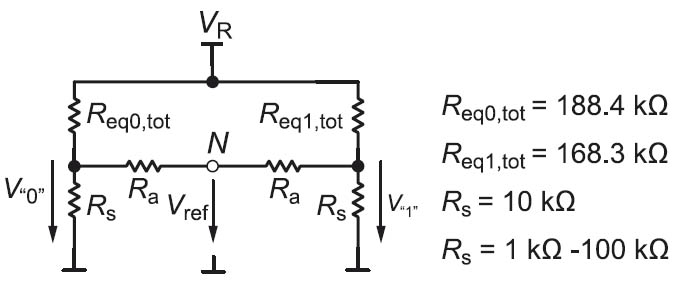
Figure 4: Simplified equivalent circuit for generating the reference voltage by using resistors and real simulation results.
The values of the used resistors Ra are not critical. To illustrate this, the total equivalent resistance connected to the two sense resistors is calculated from the voltage drops on them. After that, the effect of sweeping the value Ra on the voltages V”1”, V”0”, and Vref is investigated. Which “1” or “0” is chosen from a row does not impose any restrictions on this concept. Thus we will consider the voltages of the “1” with the highest voltage and the “0” with the lowest voltage in Figure 2. These voltages are 56.1 mV and 50,4 mV respectively which correspond to the equivalent resistances of 168,3 kΩ and 188,4 kΩ connected to the sense resistors as shown in Figure 4. The simulation results obtained by sweeping the value of Ra from 1 kΩ to 100 kΩ are shown in Figure 5. As can be seen, V”1” and V”0” are degraded especially for small values of Ra but the reference voltage stays practically constant.
Figure 6 shows the output voltages resulting from reading a row from 64 × 16 bit logical memory, which is physically 73 × 16 crossbar array after inserting the reference cells. In this simulation every ninth cell is a reference cell.
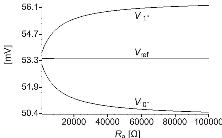
Figure 5: Simulation results of sweeping the value of Ra from 1 kΩ to 100 kΩ.
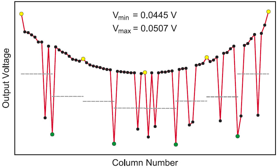
Figure 6: The crossbar array after inserting reference cells and reference generating resistors.
The parameters used are the same as in the simulation in Figure 2. The large circles indicate the positions of the reference cells and the horizontal lines represent the local reference values generated from the reference cells. It can be clearly seen, that the reference values are adjusted according to the degradation of the output voltages. This yields a reliable read operation due to the higher voltage margin between the voltage levels of the “1”s and “0”s and their corresponding reference voltage.
J. Mustafa, R. Waser
Simulation of the Near-GB Defect Chemistry in Acceptor-Doped SrTiO3
TASK
The electrical properties of acceptor-doped SrTiO3 ceramics are mainly determined by the grain boundaries (GBs). In order to obtain a detailed theoretical understanding of the GBs' electrical activity, simulation models for the defect chemistry, the electrostatics, and the electrical small-signal behaviour of the GB region are required. The simulation results have to be compared with experimental data gained by impedance spectroscopy.
APPROACH
The simulations were perform-ed in a first step along a one-dimensional axis perpendicular to the GB. A special mathematical transformation allows to adapt the position of the discrete calculation points according to the location of the largest gradients of the simulation quantities. The discretization of the Poisson-equation in combination with the system of mass action equations for all defect chemical reactions leads to a comprehensive system of nonlinear equations which is solved by the Newton-algorithm.
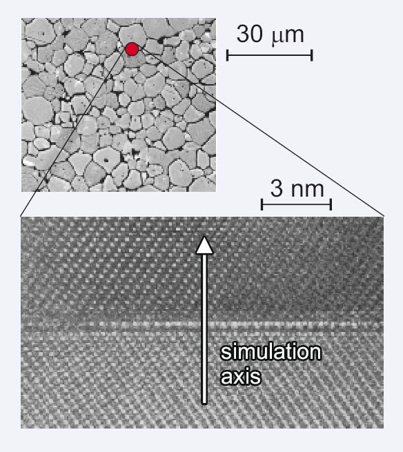
Figure 1: Upper diagram: Microsection of the etched surface of a 0.1 at% Ni-doped SrTiO3 ceramic. Lower diagram: HRTEM-diagram of the same ceramic, showing two grains separated by one GB
RESULTS
Using spatial dopant profiles as input for the simulations, local distributions of all mobile and immobile defects are calculated.
This leads to a detailed picture of the defect chemistry near the GBs which is completely different from the situation within the space-charge-free bulk. Furthermore, the spatial profiles of the band bending, the electrostatic potential, the electrical field, and the conductivity are calculated along the simulation axis.
The prediction by the simulations concerning the temperature dependence of the GB conductivity has been confirmed by impedance spectra of GB decorated SrTiO3 ceramics. Undecorated samples have been compared to Mn and Nb GB decorated samples, respectively. The transition temperature between the different activation energies of the GB conductivity has been shown to depend strongly on the kind of decoration cations.
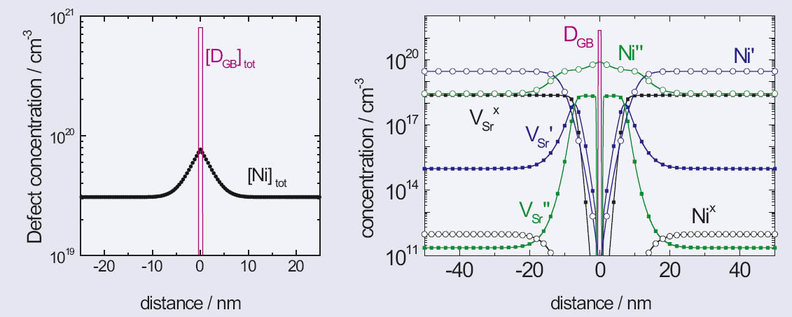
Figure 2: Left: Input parameters for the simulation: spatial profile of Ni acceptors and GB states. Right: output parameters: concentration of immobile defects
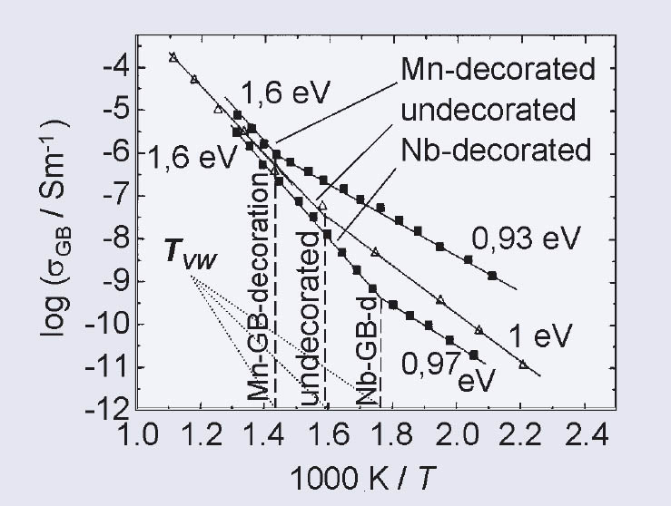
Figure 3: GB conductivity in an Arrhenius plot for undecorated, Mn- and Nb decorated SrTiO3 ceramic
R. Hagenbeck, T. Hölbling
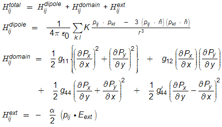
Monte-Carlo Simulation Studies
TASK
Although the principles of domain dynamics and their influence on the electrical properties of ferroelectrics are quite well understood, the details, however, are often intractable to analytical calculations due to the underlying complexity of the microstructural influences or electrical boundary conditions. So, simulations are essential to achieve information beside the experimental data. Here Monte-Carlo simulations were used to investigate the influence of defects, frequency, temperature, and interfaces on the dielectric constant and the ferroelectric properties.
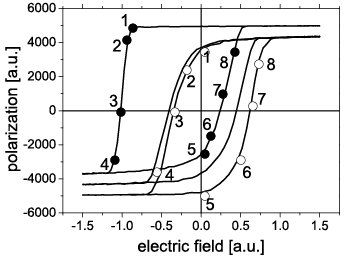
Figure 1: Failure mechanisms due to the imprint effect.
APPROACH
In this model, each ferroelectirc is made up of constant dipole moments, representing a single dipole moment of a unit cell arranged in a 2D square lattice. All 4 possible orientations in a tetragonal ferroelectric were established and 90° as well as 180° domain walls can be formed. The simulated lattice was sized from 50 x 50 to 200 x 200 cells. A distributed computing approach was used to allow the simulation of a whole in parallel. To calculate the physical behavior of the dipoles one has to define an Hamiltonian, which describes that interactions correctly. The used Hamiltonian here consists of 3 different terms. The first one describes the long-range dipole-dipole interaction, the second one penalizes the system for building up gradients by introducing a polarization gradient energy, and the last one takes the interaction of dipoles with an external electrical field into account:
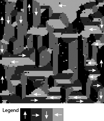
Figure 2: Non-linear voltage shift due to imprint.
This approach leads to a successfully reproduction of the ferroelectric behavior.
RESULTS
A non-linear imprint behavior was observed that has not been reported before. The whole curve of the coercive voltage shift over the elapsed time could The inclusion of randomly oriented defect dipoles results in a strong decrease of the remnant polarization and a strong back-switching effect. Simulated C-V curves showed that the variation of capacitance is due mainly to domain wall contributions. The frequency and temperature dependence were also in good agreement with experiments performed on PZT thin films. Since the motion of domain walls of the small-signal capacitance on frequency might be due to the time needed for new nucleation processes to occur, thereby limiting the domain wall contributions to the permittivity at high frequencies. The calculations also provided the evidence that nucleation and growth dynamics alone can cause an imprint-like effect in ferroelectric thin films. Monte-Carlo simulations proved to be a viable tool to develop further insight into physics of ferroelectrics.
- [1] D. Bolten, U. Boettger and R. Waser, Jap. J. Appl. Phys., Vol. 41 (11B), (2002).
- [2] D. Bolten, U. Boettger and R. Waser, J. Appl. Phys., Vol. 93, 2890 (2002).
- [3] D. Bolten, U. Boettger and R. Waser, Appl. Phys. Lett. 84, 2379 (2004).
D. Bolten, P. Schorn, U. Böttger, R. Waser