Chemical Routes Towards Thin Films: CSD and MOCVD
The thin film deposition techniques available in the laboratories in Aachen and Jülich cover the two main chemical methods for the growth of electroceramic thin films: the chemical solution deposition (CSD) and the metal organic chemical vapor deposition (MOCVD) method.
Chemical Solution Deposition (CSD)
In the CSD process a solution containing organic compounds of the metal ions is deposited on the substrate by dip, spray or spin coating. The wet film is either firstly pyrolyzed or directly crystallized. A sequence of deposition and heat treatment procedures followed by a final post annealing step results in the crystalline film.
The CSD method is a very flexible technique of high reproducibility. With optimized process parameters, dense and homogeneous crystalline thin films of high quality have been grown. They are suitable for integration on the micron size scale as thin film capacitors in MMICs or as piezoelectric elements in MEMs.
The CSD tools installed in the cleanroom of the IWE are part of the aixACCT laboratory group. The equipment is designed for wafer sizes up to 150 mm:
- Spin coaters (BLE)
- Spray coater (Samco)for conformal coverage of 1 μm x 1 μm trench structures
- Hot plates, Tmax = 800 K
- Diffusion furnaces (Centrotherm) and a Rapid Thermal Processing system (Steag AST)
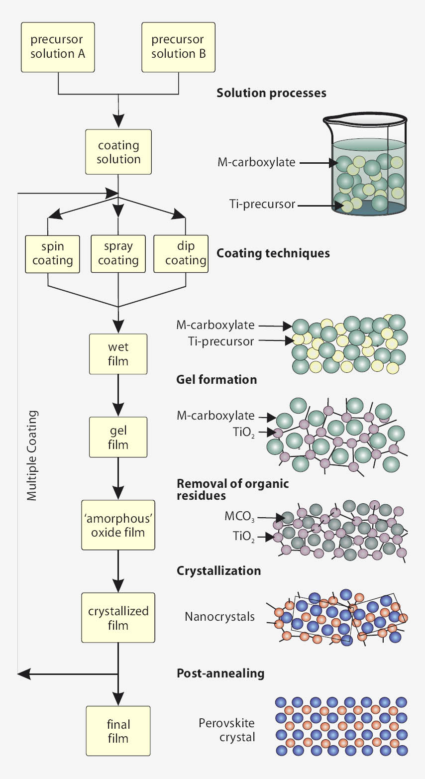
Figure 1: Flow chart of the principle steps of the chemical solution deposition (CSD) method
Metal Organic Chemical Vapor Deposition (MOCVD)
MOCVD methods are considered as primary deposition techniques for perovskite oxide films on the sub-micron size scale for high-k or ferroelectric memory devices due to their high deposition rates, amenability to large wafer size scaling, and their potential for a high degree of film thickness conformality over complex device topographies.
Two MOCVD systems are installed in the cleanroom of the EKM/IFF:
- a prototypic production MOCVD reactor based on an AIX-2600G3 planetary reactor which can handle up to five 6 inch wafers simultaneously. In cooperation with the Aixtron AG the system is used for the evaluation of MOCVD processes which are reliable enough for large scale production.
- a research reactor based on an Aixtron AIX-200 horizontal reactor core for single 2 inch wafers. The system is used for fundamental studies of the MOCVD process and for the test of new components, especially new injection systems.
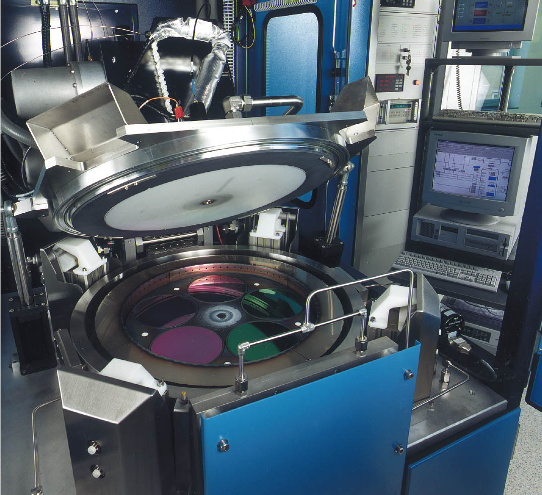
Figure 2: MOCVD planetary reactor AIX-2600G3 from the Aixtron AG which can handle five 6 inch wafers simultaneously
Thin Film Integration Technology
The cleanroom facilities in Aachen and Jülich provide a broad spectrum of equipment for the integration of electroceramic thin films into semiconductor devices.
The tools, which are designed for a 6" wafer line, enable the processing of structures with lateral dimensions on the micron scale. The equipment in the cleanroom in Aachen is part of the aixACCT laboratory group. The thin film deposition methods (CSD and MOCVD) are described in a separate article while the next two pages focus on the process steps relevant for integration: photolithography, metallization, thermal processing, dry etching and back-end processing techniques.
Photolithography
Photolithographic steps are involved in various processes: structuring of the bottom and top electrode and the ceramic thin film by means of dry etching, wet etching and lift-off techniques.
The photolithography facilities comprise:
- Quick-dump rinsers
- Ultrasonic baths
- Spin coaters
- Hot plates
- Two MA6 mask aligners (Karl Süss), one with additional back side exposure
- Wafer inspection microscopes with image processing software
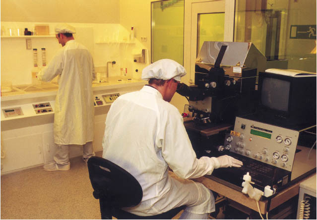
Figure 1: Lithography area
Metallization
The activities performed on metallization-related topics are twofold:
First, the technological aspect of the metallization processes focuses on the preparation of reproducible, high-quality bottom electrode stacks deposited on silicon substrates.
Second, the research interests in metallization techniques cover the evaluation of new compositions for conductive, process-compatible bottom electrode stacks. Additional studies are performed on the influence of the electrode microstructure on the growth process and the morphological and electrical properties of the electrode / thin film / electrode structures.
Available metallization facilities cover both areas of technology, i.e. the high throughput production tool and the flexible research equipment.
- Sputtering cluster tool (Ardenne) which can handle six 4" or four 6" wafers equipped with three magnetrons (two DC, one RF) and two back side heaters. The whole cluster tool consists of the sputtering system, an automatic handler for 6" wafers and an e-beam evaporation chamber for single 6" wafers
- Two UHV-sputtering systems (FZJ) for wafer sizes of 2" equipped with DC and RF magnet-rons and substrate heaters. Available target materials cover 14 metals, alloys, and oxides like e.g. ZrO2, Al2O3, SiO2
- Electron beam evaporation system for single 4" wafers
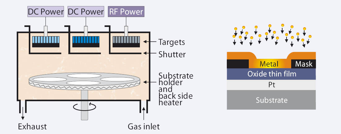
Figure 2: Schematic sketch of sputtering tool and lift-off process
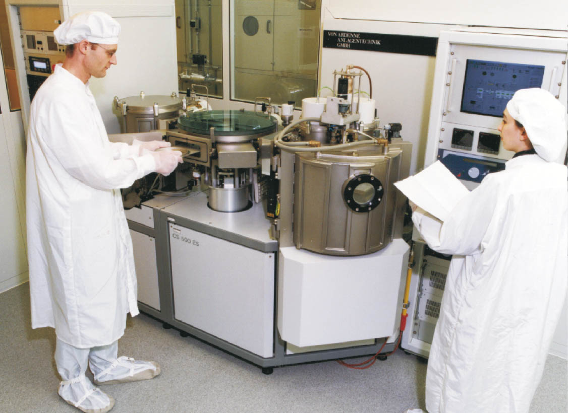
Figure 3: Sputtering cluster tool
Thermal Processing
Thermal processing steps involved are oxidation of silicon substrates, annealing of adhesion layers, crystallization of electroceramic thin films and forming gas annealing of completely integrated devices.
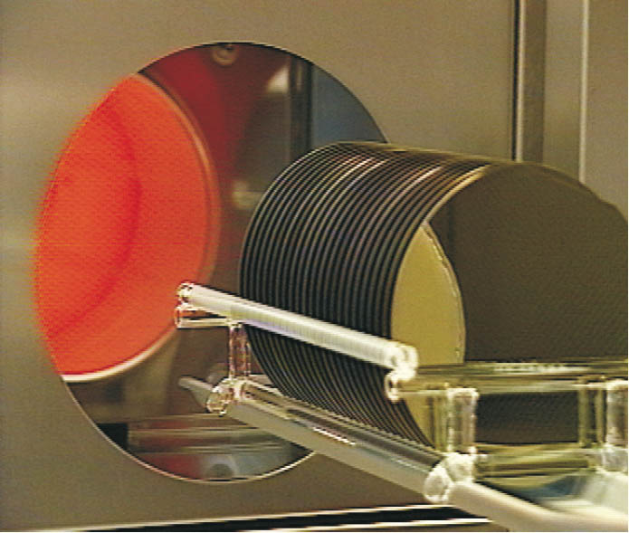
Figure 4: Oxidation of 6" silicon wafers
The various tasks require different thermal processing systems with respect to the heating rate and desired gas atmospheres. In order to avoid contaminations separate furnaces are available for the silicon processes and the thin film heat treatment with respect to Pb- and Bi-free and Pb- and Bi-containing compounds, respectively.
- Diffusion furnace (Centrotherm) with two tubes for 4" wafers
- Diffusion furnace (Centrotherm) with two tubes for 6" wafers, one equipped with a hydrogen burner for Si oxidation
- Rapid thermal process system (Steag AST) for single 6" wafers with gas lines for O2, N2 and N2/H2
Dry Etching
Know-how about dry etching process parameters for oxide thin films and metallization layers is mandatory for a successful realization of devices based on electro-ceramic thin films as for example integrated thin film multilayer capacitors or piezoelectric microrelays.
For fundamental as well as technological research studies two dry etching systems are available:
- Reactive ion etching system (RIE) (Roth & Rau) with an ECR plasma source and a substrate heater / chiller for 4" and 6" wafers
- Reactive ion beam etching system (RIBE) (Oxford Ionfab 300 plus) with a substrate heater / chiller for 6" wafers and equipped with an energy dispersive quadropole mass spectrometer (Hiden EQP) for the analysis of volatile reaction products
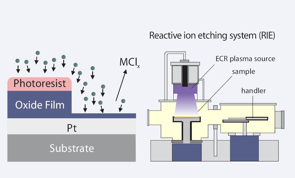
Figure 5: Schematic sketch of the RIE system and the etching process
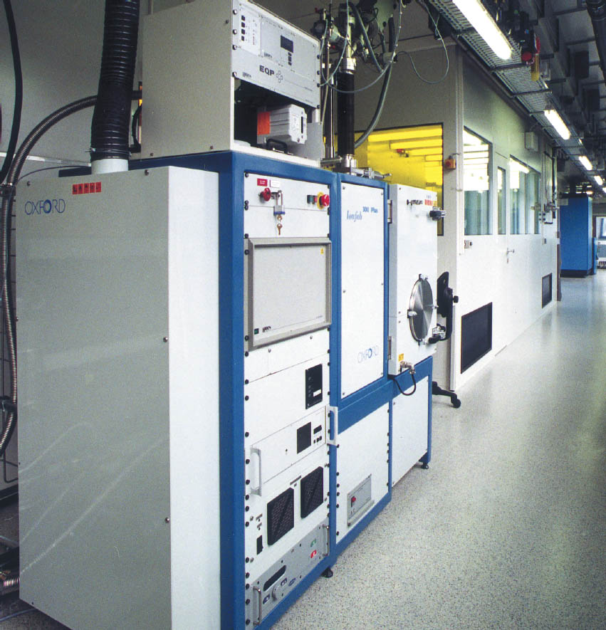
Figure 6: Reactive ion beam etching system with quadrupole mass spectrometer
Mechanical Techniques
The facilities of the 6" wafer line for integration of electroceramic thin films are complemented by the standard back-end technologies wafer sawing and bonding.
- Automatic wafer saw (Disco)
- Ultrasonic wafer bonder (Kulike-Soffa)
Dry Etching of (Ba, Sr)TiO3 Thin Films
TASK
An important issue of the integration of electroceramic thin films into modern micro-electronics is the patterning process. Typically, this is per-formed by means of reactive ion etching (RIE), because of its high degree of anisotropy. RIE represents the method of choice for patterning features in the submicron range com-pared to the isotropic character of wet chemical etching.
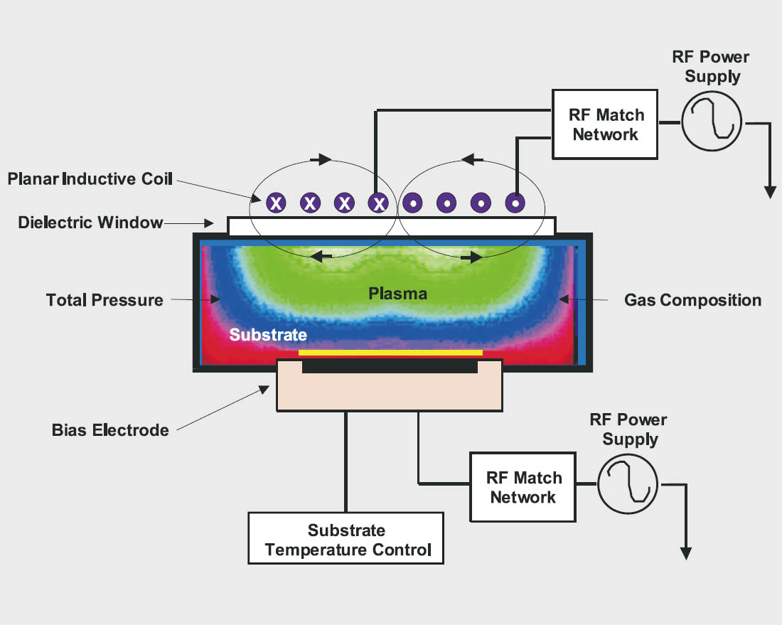
Figure 1: Schematic illustration for the Transformer Coupled Plasma (TCP) reactor showing the planar source coil and the temperature controlled wafer electrode (Lam Research).
APPROACH
Reactive Ion Etching of Ba0.7Sr0.3TiO3 (BST) - thin films was studied by using a Lam TCPTM 9400SE high density, low pressure plasma reactor in a cooperation with Lam Research. A designed experiment for the variables was performed etch chemistry, total pressure, coil power, bottom power, and gas flow. Etch results were characterized using SEM with respect to etch rate, selectivity to photoresist mask and SiO2 substrate, etch profile, sidewall redepositions (fences), and residues of etch products.
RESULTS
One major challenge of etch-ing BST is the formation of typically non-volatile etch products. If these products redeposit on sidewalls of the patterned masks fences are build up that have deteriorating impact on further pro-cessing. To meet the goals of (1) a high etch rate, (2) a steep sidewall slope and (3) a clean wafer surface (without residues and fences), a suitable process has to operate at low pressures, with a high plasma density and ion energy. Reactive gas addition is mandatory. An optimized etch process was established with an etch rate of 70 nm/min and a profile slope of about 80°.
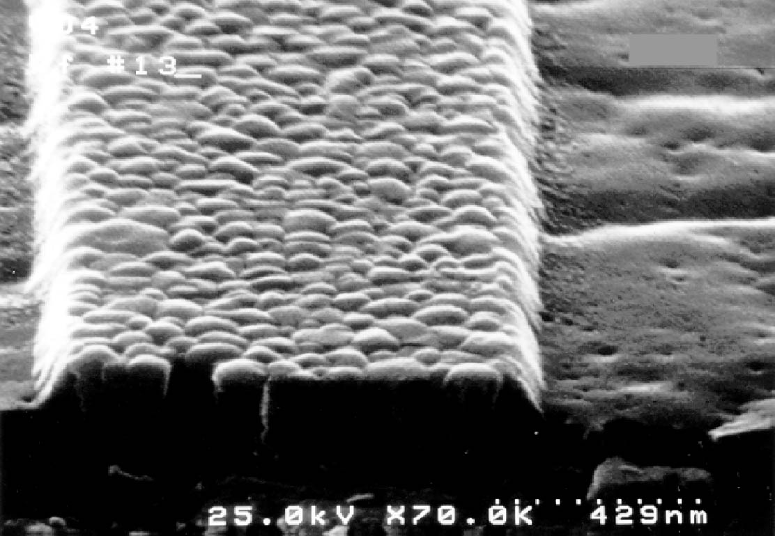
Figure 2: Cross section of an etched BST thin film
S. Schneider